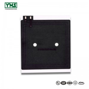
Original Factory China OEM ODM PCB Assembly and PCB Manufacturer with SMT DIP Service
We thinks what clients think, the urgency of urgency to act from the interests of a client position of theory, allowing for greater quality, lessen processing costs, price ranges are much more reasonable, won the new and outdated shoppers the support and affirmation for Original Factory China OEM ODM PCB Assembly and PCB Manufacturer with SMT DIP Service, Our products and solutions are widely recognized and reliable by users and can meet continuously changing economic and social needs.
We thinks what clients think, the urgency of urgency to act from the interests of a client position of theory, allowing for greater quality, lessen processing costs, price ranges are much more reasonable, won the new and outdated shoppers the support and affirmation for China PCB Assembly Services, SMT DIP, We adhere to the honest, efficient, practical win-win running mission and people-oriented business philosophy. Excellent quality, reasonable price and customer satisfaction are always pursued! If you are interested in our products, just try to contact us for more details!
Printed Circuit Board Introduction
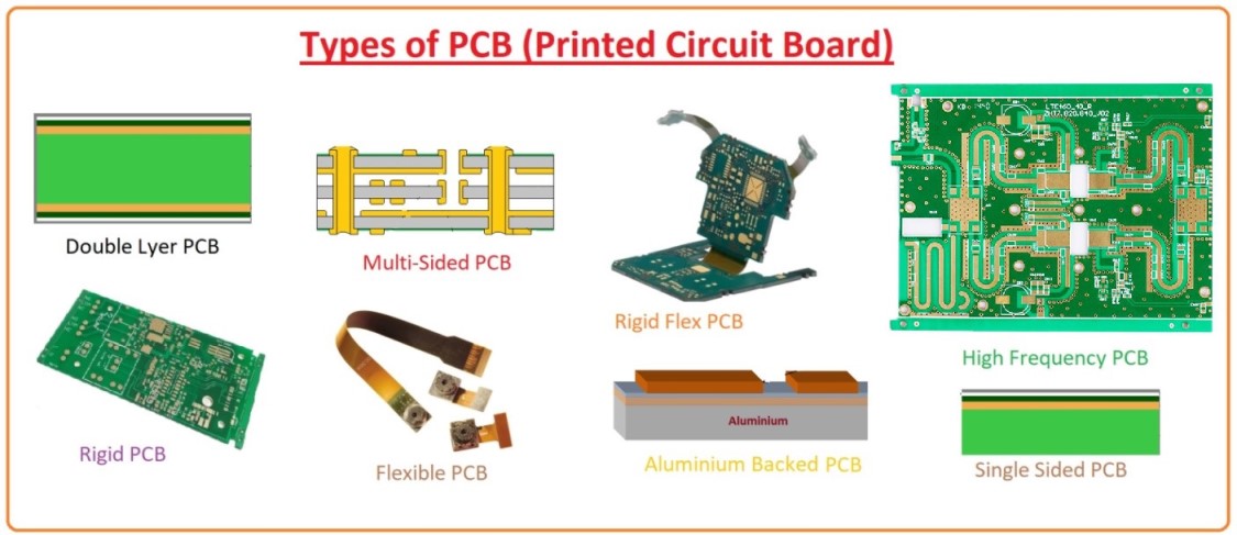
A printed circuit board (PCB) mechanically supports and electrically connects electrical or electronic components using conductive tracks, pads and other features etched from one or more sheet layers of copper laminated onto and/or between sheet layers of a non-conductive substrate. Components are generally soldered onto the PCB to both electrically connect and mechanically fasten them to it.PCBs can be single-sided (one copper layer), double-sided (two copper layers on both sides of one substrate layer), or multi-layer (outer and inner layers of copper, alternating with layers of substrate). Multi-layer PCBs allow for much higher component density, because circuit traces on the inner layers would otherwise take up surface space between components. The rise in popularity of multilayer PCBs with more than two, and especially with more than four, copper planes was concurrent with the adoption of surface mount technology.
YMS Normal PCB manufacturing capabilities:
| YMS Normal PCB manufacturing capabilities overview | ||
| Feature | capabilities | |
| Layer Count | 1-60L | |
| Available Normal PCB Technology | Through hole with Aspect Ratio 16:1 | |
| buried and blind via | ||
| Hybrid | High Frequency Material such as RO4350B and FR4 Mix etc. | |
| High Speed Material such as M7NE and FR4 Mix etc. | ||
| Material | CEM- | CEM-1;CEM-2;CEM-4;CEM-5.etc |
| FR4 | EM827, 370HR, S1000-2, IT180A, IT158, S1000 / S1155, R1566W, EM285, TU862HF,NP170G etc. | |
| High Speed | Megtron6, Megtron4, Megtron7,TU872SLK, FR408HR,N4000-13 Series,MW4000,MW2000,TU933 etc. | |
| High Frequency | Ro3003, Ro3006, Ro4350B, Ro4360G2, Ro4835, CLTE, Genclad, RF35, FastRise27 etc. | |
| Others | Polyimide, Tk, LCP, BT, C-ply, Fradflex, Omega , ZBC2000,PEEK,PTFE,ceramic-based etc. | |
| Thickness | 0.3mm-8mm | |
| Max.copper Thickness | 10OZ | |
| Minimum line Width and Space | 0.05mm/0.05mm(2mil/2mil) | |
| BGA PITCH | 0.35mm | |
| Min mechanical Drilled Size | 0.15mm(6mil) | |
| Aspect Ratio for through hole | 16:1 | |
| Surface Finish | HASL, Lead free HASL,ENIG,Immersion Tin, OSP, Immersion Silver, Gold Finger, Electroplating Hard Gold, Selective OSP,ENEPIG.etc. | |
| Via Fill Option | The via is plated and filled with either conductive or non-conductive epoxy then capped and plated over(VIPPO) | |
| Copper filled, silver filled | ||
| Registration | ±4mil | |
| Solder Mask | Green, Red, Yellow, Blue, White, Black, Purple, Matte Black, Matte green.etc. | |


