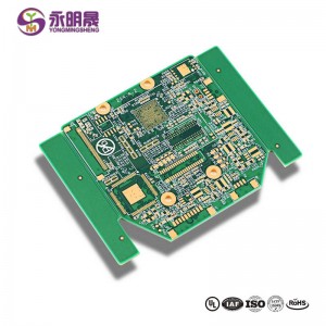
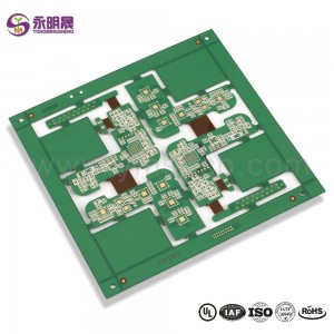
Top Grade China 2layer Shengyi Fr4 Enig 2u Pwr LED PCB Circuit PCB
We also supply merchandise sourcing and flight consolidation companies. We now have our very own manufacturing facility and sourcing business. We could present you with almost every kind of product relevant to our solution array for Top Grade China 2layer Shengyi Fr4 Enig 2u Pwr LED PCB Circuit PCB, And there are also many foreign friends who came for sight seeing, or entrust us to buy other stuff for them. You are most welcome to come to China, to our city and to our factory!
We also supply merchandise sourcing and flight consolidation companies. We now have our very own manufacturing facility and sourcing business. We could present you with almost every kind of product relevant to our solution array for China Motherboard PCB, Pwr LED PCB, Our company warmly invites domestic and overseas customers to come and negotiate business with us. Let us join hands to create a brilliant tomorrow! We are looking forward to cooperating with you sincerely to achieve a win-win situation. We promise to try our best to provide you with high quality and efficient services.
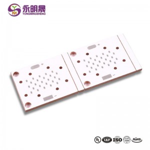
Copper PCB
Copper-based circuit board is one of the most expensive metal substrates, and its thermal conductivity is many times better than that of aluminum or iron substrates.Suitable for high frequency circuit and high and low temperature variation area as well as precision communication equipment heat dissipation and building decoration industry.
In general, the surface finish of the copper-base circuit printed board is impregnated with gold, plated with silver, HAL, OSP, etc.
The circuit layer of copper core PCB needs to have a large carrying capacity, so thick copper foil should be used. The thickness is generally between 35 and 280 meters.Thermal insulation layer is its core technology.Copper base PCB.The core thermal conductivity module consists of a mixture of alumina and silicon powder and epoxy resin.Low heat resistance (0.15), excellent viscoelasticity, and heat resistance aging.Able to withstand mechanical and thermal stress.
The metal base is the supporting component of copper core PCB, which is required to have high thermal conductivity. It is usually based on copper PCB, suitable for traditional mechanical drilling, punching, cutting and other processing. The metal layer (block) mainly plays the role of heat dissipation, shielding, covering or grounding.Because of the characteristics of copper and aluminum and the different processing performance of the corresponding PCB, copper based PCB has more performance advantages than aluminum core PCB.
The thermal conductivity of a copper base is twice that of aluminum.The higher the thermal conductivity, the higher the heat transfer efficiency and the better the heat dissipation performance.
Copper base can be processed into metallized holes, aluminum base is not allowed.The metallized mesh must be the same network so that the signal has good grounding performance, and secondly, the copper itself has weldability, finally completing the structural part of the design.Installation is optional.
The copper substrate of the copper substrate can be etched into a fine pattern and processed into a convex boss shape. The components can be directly connected to the convex boss to achieve good grounding and heat dissipation effect.
Due to the difference in the elastic modulus between copper and aluminum (the elastic modulus of copper is about 121,000 MPa) and the elastic modulus of aluminum is 72,000 MPa), the corresponding warping and shrinkage of the copper substrate will be smaller than the warping and shrinkage of the aluminum substrate, so the overall performance is better and stable.
Rules for designing copper substrates: due to the thickness of the copper substrates, the minimum borehole radius must be 0.4mm.The wire width is determined according to the thickness of the copper foil on the copper substrate.The thicker the copper foil, the wider the line.The minimum spacing must be larger.
Copper base Board production process
Provide the copper plate have pretreated
UV ink is printed on the bending part of copper plate
The surface of copper plate is browned by using browning liquid
Press and drill copper plate covered with UV ink
Electroplate the first finished product
Make outer layer on copper plate
Solder mask printing on copper substrate
V – CUT the second finished product
The bending position of copper plate is surface treated and the finished product is obtained
Check up case ,packing and shipping
You May Like:
1、Gold, silver and copper in PCB
2、Why is the copper thickness in PCB an ounce
3、Copper PCB and aluminum PCB difference


