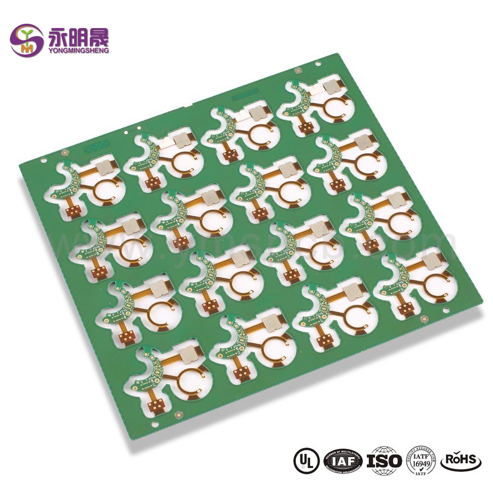
Double sided pcb Normal pcb Lead free HASL Counterbore Manufacturer | YMS PCB
HAL(Lead Free), the full name is Hot Air leveling with Lead Free. Compared with HASL, the main difference for HAL(Lead Free) is the element of material which do not contain Lead(Pb), so it’s RoHS Compliant and it’s much more popular and widely used in wax soo saarka PCB.
HAL(Lead Free) requires higher run temperatures for lead free solder and longer contact time, the production cost for HAL(Lead Free) is slightly higher than HASL(Tin/Lead).
The manufacturing process of HAL(Lead Free) is similar to HASL(Tin/Lead), the circuit boards will be submersed in molten solder(Lead Free). This solder will cover all the exposed copper surfaces. Upon retraction from the solder, high pressure hot air is blown over the surface through air knives, this levels the solder deposit and removes the excess solder from the surface of printed circuit boards.
Hordhac Wareegtada Guddiga Wareegga
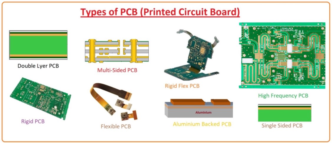
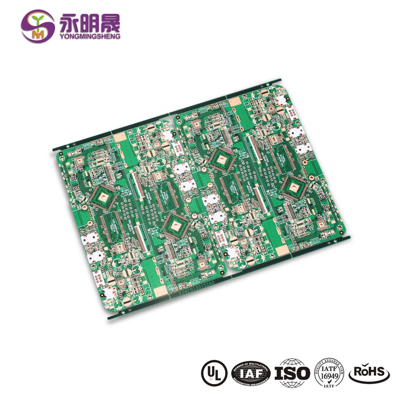
Guddiga Wareega ee Daabacan ee Caadiga ah: Most PCBs for simple electronics are simple and composed of only a single layer. More sophisticated hardware such as computer graphics cards or motherboards can have 2 or multiple layers, sometimes up to twelve.
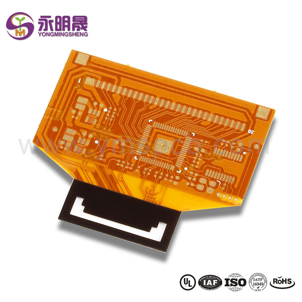
A printed circuit board (PCB) mechanically supports and electrically connects electrical or electronic components using conductive tracks, pads and other features etched from one or more sheet layers of copper laminated onto and/or between sheet layers of a non-conductive substrate. Components are generally soldered onto the PCB to both electrically connect and mechanically fasten them to it.PCBs can be single-sided (one copper layer), double-sided (two copper layers on both sides of one substrate layer), or multi-layer (outer and inner layers of copper, alternating with layers of substrate). Multi-layer PCBs allow for much higher component density, because circuit traces on the inner layers would otherwise take up surface space between components. The rise in popularity of multilayer PCBs with more than two, and especially with more than four, copper planes was concurrent with the adoption of surface mount technology.
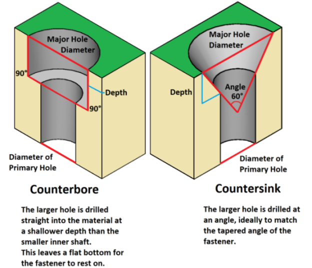
What is the difference between a Countersink and a Counterbore?
YMS Awoodda wax soo saarka PCB ee caadiga ah:
| Guudmarka awooda wax soosaarka PCB-ga ee YMS | ||
| Muuqaalka | awoodaha | |
| Tirinta Lakabka | 1-60L | |
| Teknoolojiyada PCB ee Caadiga ah | Iyada oo loo marayo godka Qaybta Aspect 16: 1 | |
| aasay oo indho la 'via | ||
| Iskujir | Waxyaabaha Frequency High sida RO4350B iyo FR4 Mix iwm. | |
| Waxyaabaha Xawaaraha Sare leh sida M7NE iyo FR4 Mix iwm. | ||
| Waxyaabaha | CEM- | CEM-1; CEM-2 ; CEM-4 ; CEM-5. iyo wixii la mid ah |
| FR4 | EM827, 370HR, S1000-2, IT180A, IT158, S1000 / S1155, R1566W, EM285, TU862HF, NP170G iwm | |
| Xawaare sare | Megtron6, Megtron4, Megtron7, TU872SLK, FR408HR, N4000-13 Series, MW4000, MW2000, TU933 iwm | |
| Joogtaynta Sare | Ro3003, Ro3006, Ro4350B, Ro4360G2, Ro4835, CLTE, Genclad, RF35, FastRise27 iwm | |
| Qaar kale | Polyimide, Tk, LCP, BT, C-ply, Fradflex, Omega, ZBC2000, PEEK, PTFE, dhoobada ku saleysan iwm | |
| Dhumucdiisuna | 0.3mm-8mm | |
| Dhumucda Maxaxda | 10OZ | |
| Ballaaran khadka ugu yar iyo Booska | 0.05mm / 0.05mm (2mil / 2mil) | |
| GAROONKA BGA | 0.35mm | |
| Min Qiyaas ahaan qodan Farsamo | 0.15mm (6mil) | |
| Saamiga saamiga illaa daloolka | 16 : 1 | |
| Dhammeystirka dusha sare | HASL, Lead free HASL, ENIG, Immersion Tin, OSP, Immersion Silver, Finger Gold, Electroplating Gold Gold, Selective OSP , ENEPIG.etc. | |
| Via Buuxi Xulashada | Khadka la mariyo ayaa lagu dhajiyay oo lagu buuxiyay epoxy tabin ama tabin la'aan ah ka dibna la daboolay oo la dul saaray (VIPPO) | |
| Naxaas la buuxiyey, lacagna la buuxiyey | ||
| Diiwaangelinta | M 4milyan | |
| Maaskaro Alxan | Cagaar, Casaan, Jaale, Buluug, Caddaan, Madoow, Midabbo, Matte Madow, Matte green. Iwm. | |
Waxaad laga yaabaa:
1, Kooban arrimaha u baahan fiiro gaar ah in alxanka guddiga circuit
4、Waa maxay baaritaanka guddiga qaawan?
5. Waa maxay naqshadaynta PCB ee soo noqnoqda sare
Baro wax badan oo ku saabsan alaabta YMS


