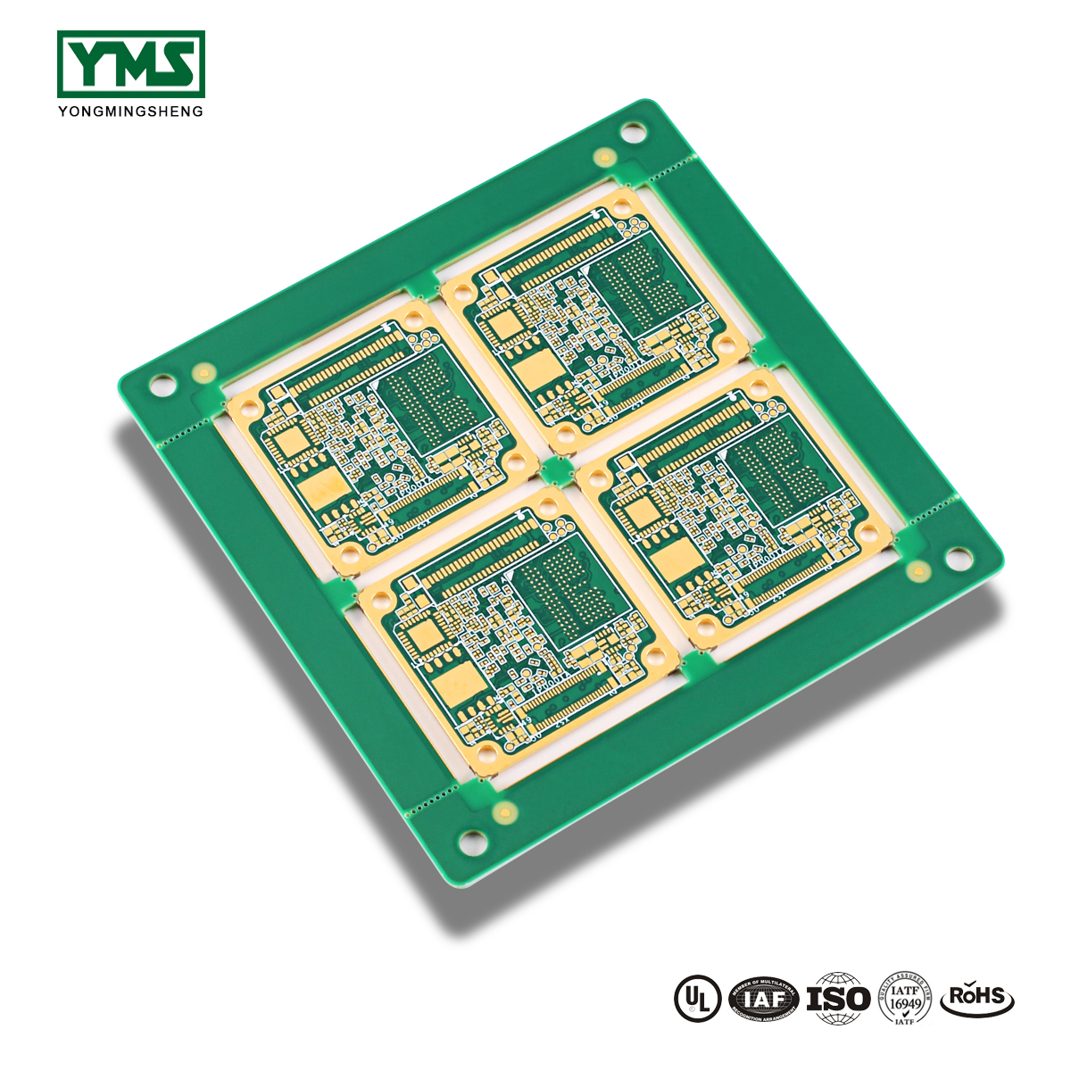
OEM China Lead Free Hasl - 2Layer Lead free Hasl Green soldermask Board | YMS PCB – Yongmingsheng
OEM China Lead Free Hasl - 2Layer Lead free Hasl Green soldermask Board | YMS PCB – Yongmingsheng Detail:
The production method of 2 Layer PCB is generally made by inner layer pattern first, and then made into single or double side substrate by printing etching method, which is incorporated into the specified layer, and then heated, pressurized and glued. As for the subsequent drilling, it is the same as the plating through hole method of double panel. These basic manufacturing methods have not changed much since the 1960s, but as materials and process techniques (e.g., pressing and bonding techniques, improvements to the glue residue produced by drilling, film) have matured, the properties attached to the multilayer have become more diverse.
Product detail pictures:

Related Product Guide:
High Density Interconnect(HDI) PCBs Market Analysis, Forecast Of Business Revenue, Size, Leading Competitors and Growth Trends | Fingerprint Lock Rigid-Flexible Pcb
High-Density Interconnect (HDI) PCB Market 2018 Size, Volume Analysis, Industry Profiles and Revenue 2026 | Hdi Pcb
We emphasize development and introduce new products into the market every year for OEM China Lead Free Hasl - 2Layer Lead free Hasl Green soldermask Board | YMS PCB – Yongmingsheng , The product will supply to all over the world, such as: America, London, Brasilia, All styles appear on our website are for customizing. We meet up to personal requirements with all products of your very own styles. Our concept is to help presenting the confidence of each buyers with the offering of our most sincere service, and the right product.
Goods just received, we are very satisfied, a very good supplier, hope to make persistent efforts to do better.
Write your message here and send it to us


Board2.jpg)


