What is PCB Stack-up?
The stack-up defines the number of layers, the distance between layers, and the materials used in the PCB fabrication.
The objective of the PCB stack-up design process is to select suitable materials, and layer them to achieve optimal signal performance and power integrity at the lowest PCB cost.
The performance of a circuit board assembly is significantly dependant on the design of the PCB stack-up.
Consideration factors in stack-up design:
· the number of layers needed
· the arrangement of layers
· layer material
· routing and vias
The PCB Stack-up Structure
The PCB stack-up is the foundation upon which all design components are built. Therefore, a poorly designed PCB stack-up with improperly selected materials can adversely affect the performance of the circuit assembly in the way of signal transmission, power delivery, manufacturability, and reliability.
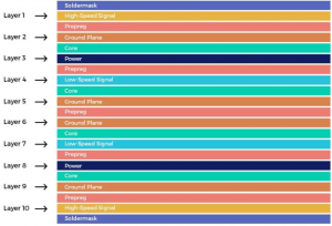
A typical PCB stack-up is constructed from multiple alternating layers of core, prepreg, and copper foil materials heat-pressed and glued together.
The core material (a cured fiberglass-weave material with epoxy resin) is a thin electrical insulator (dielectric) with copper-clad foils bonded to both sides. So, the dielectric acts as an insulation layer between the copper foils. The internal copper form the signal, power, and ground planes (layers) in the PCB. Prepreg binds the core layers and operates as insulation between core layers.
During the PCB manufacturing process, the layer arrangement of core and prepreg layers are laminated together with a top and bottom copper layer. The PCB is formed using heat and pressure to bind all the different (PCB stacks) layers together.
The number of layers needed (layer count)
Among the several factors that need to be considered when determining the number of layers needed, the most pivotal are:
· power/ ground / signal layer requirements
· board complexity
· component density
· component package types
To obtain the best signal integrity of the channel for high channel count /high channel density devices, channel routing will probably need to be accommodated with blind vias in addition to layer arrangements.

Layer arrangement
In the layer stack up, the power plane is usually placed directly next to a ground layer to maintain signal performance and signal robustness. And, to minimize the total layer count the power plane is shared to the extent possible.
Spacing between adjacent signal layers should be increased. However, this can impact the overall thickness of the PCB when large separations are present.
For high-speed traces, the routing layer should be planned during stack-up design, where high-speed signals are routed on minimum thickness microstrips.
Dielectric Materials
The most popular Dielectric material is FR4 and may be in the form of core or prepreg (pre impregnated) material. The core material is thin dielectric (cured fibreglass epoxy resin) with copper foil bonded to both sides. For instance: Isola’s FR406 materials – include 5, 8, 9.5, 14, 18, 21, 28, 35, 39, 47, 59 and 93 MIL cores. The copper thickness is typically ½ to 2 oz (17 to 70 um).
The prepreg material is thin sheets of fibreglass impregnated with uncured epoxy resin which hardens when heated and pressed during the PCB fabrication process. Isola’s FR406 materials – include 1.7, 2.3, 3.9 and 7.1 MIL prepregs that may be combined to achieve the desired prepreg thickness.
The most common stackup called the ‘Foil Method’ is to have prepreg with copper foils bonded to the outside on the outer most layers (top and bottom) then core alternating with prepreg throughout the substrate.
Conclusion
At YMS, we’ve designed everything from simple 2-layer boards to complex HDI PCBs for digital and analog systems. We know PCB layer stackup design and how to ensure your board operates as you intend. We're here to help electronics companies design modern PCBs and create cutting-edge technology. We are Chinese PCB manufacturer, and we'll make sure your next layout is fully manufacturable at scale. Contact YMS for a consultation.
Learn more about YMS products
Read more news
Post time: Jun-28-2022


