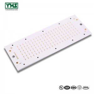
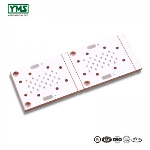
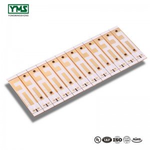
The holes on the printed circuit board are generally divided into those with copper holes and those without copper holes, which are mainly used for positioning and installation, and generally belong to relatively large holes, more than 0.8mm. And the through hole generally belongs to the plug-in or through hole;
The most common hole on PCB should be through hole (through hole), the plug hole aperture is larger than through hole size, generally more than 0.5, based on inserted capacitor, resistance, socket and other components.
The over hole is mainly used for conducting, the aperture is generally small, the common aperture is less than 0.3, with the increase of precision plate, product function requirements increase, the number of PCB layers, the aperture is also increasingly small, the minimum aperture is 0.1mm. Laser drilling is needed.
In order to conduct through the hole, copper skin is needed to conduct, so the thickness, saturation and quality of copper hole naturally become the key to the later work of circuit board.
Generally speaking, the thickness of hole copper wall of PCB is required to be 10um to 20um, and the current requirement of products with larger current is more than 25.4um.
Since the hole copper is electroplated in the later stage, unlike the surface copper which comes with its own raw materials, the quality of the hole copper depends on the production and processing of the circuit board factory in the later stage. Electroplating time, quality of electroplating line, etc.
Generally, the saturated hole copper plate, hope to give enough time on the electroplating line, otherwise it is easy to cause the hole copper is not enough, in addition, the copper ball is also required to clean quickly, otherwise it will cause blister.
Not enough hole copper will cause circuit interruption or burning of the circuit board later working process.
The finished copper thickness of PCB is made up of the base copper thickness of PCB plus the final thickness of board electricity and figure electricity. That is to say, the copper thickness of PCB is larger than that of PCB.
However, all the hole copper thickness of our PCB is completed by electroplating in two processes, that is, the thickness of hole copper plating on the whole board and the copper thickness of pattern electroplating.
The thickness of the conventional finished product is 1OZ copper, and the hole copper is in accordance with IPC grade II standard. The thickness of the first copper (full plate plating) is usually 5-7um, and the thickness of the second copper (graphic plating) is 13-15um.
Therefore, the copper thickness of the hole is between 18 and 22um. With the loss caused by etching and other reasons, the final copper thickness of the hole is around 20um.
Standard requirements for copper thickness in hole (IPC-6012b, GJB 362a-96, QJ3103-99)
Through hole electroplating is a very important link in PCB manufacturing process. To provide electrical connection for different levels of conductive metal, copper with good electrical conductivity should be plated on the hole wall of the through hole.
With the increasingly fierce competition of terminal products, it is bound to put forward higher requirements on the reliability of PCB products, and the thickness of the through hole electroplating layer has become one of the items to measure the reliability of PCB.
One of the important factors affecting the copper thickness of PCB hole is the deep plating ability of PCB.
The uniformity of copper coating thickness is an important index to evaluate the through-hole effect of PCB plating. In PCB industry, deep plating capacity is defined as the ratio of the copper coating thickness of the hole center to the copper coating thickness of the hole mouth.
In order to better describe the deep plating capacity, also often used plate thickness aperture ratio, that is, thickness diameter ratio.
PCB board is not too thick and the aperture is larger, the potential distribution in the electroplating process is more uniform, the ion diffusion degree in the hole is better, the electroplating solution's deep plating capacity value is often larger.
On the contrary, when the ratio of thickness to diameter is higher, the hole wall will show the phenomenon of "dog bone", (the phenomenon of thick copper at the orifice and thin copper at the center of the hole), and the plating solution has a poor ability of deep plating.
High depth plating capability is very important for electroplating.This is also a lot of printed circuuit board factory to solve the manufacturing process problem.
High depth plating capability has the following advantages:
1. Improve reliability assurance
The improvement of uniformity of the electroplating copper layer thickness of the hole wall provides a better guarantee for PCB in the subsequent surface mount and the cold and heat shock during the use of terminal products, so as to avoid early failure problems, prolong the service life of products and improve the high reliability of products.
2. Improve production efficiency
Electroplating process is usually the bottleneck of manufacturing process. The improvement of deep plating capacity can shorten electroplating time and improve productivity and efficiency.
3. Reduce manufacturing costs
PCB factories generally believe that if the deep plating capacity is increased by 10% from the original, at least 10% of the material cost can be reduced. The direct income of this item is in million yuan/year, not to mention a series of indirect benefits brought by the improvement of product quality.
Searches related to circuit board
Post time: Sep-05-2019


