Chinese PCB manufacturer tells you
What is the difference between a double-layer PCB and a single-layer PCB?
The difference between 1:
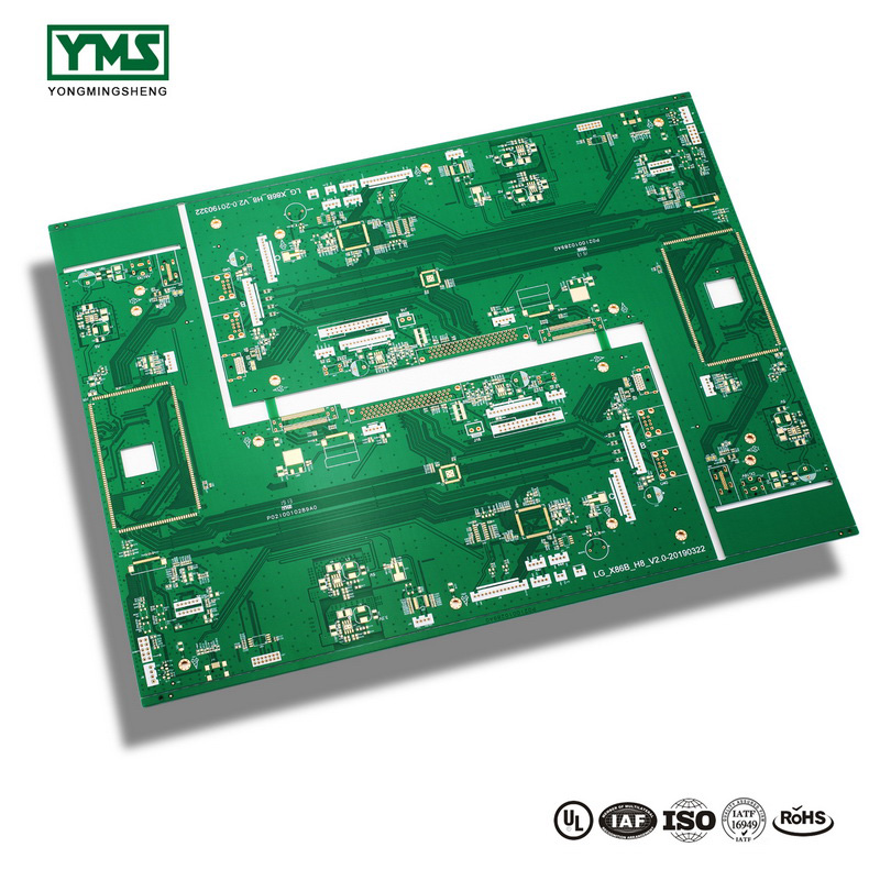
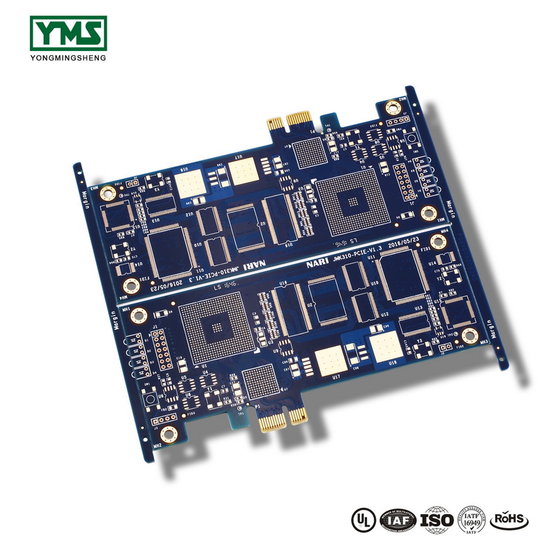
The single-layer PCB is only on one side of the PCB, while the double-layer PCB can be connected between two sides of the PCB with holes through the middle.
The difference between 2:
Parameters of double-layer PCB: Double-layer PCB production and single-layer PCB in addition to the production process is not the same, and also one more copper sinking process, that is, the process of the double-layer circuit.
A. The single-layer printed circuit board usually adopts single-layer copper-clad laminate, and uses the screen printing method or photogenic imaging method to make corroded circuit pattern on the copper surface. The redundant copper foil is removed by chemical etching to form conductor pattern.
2. Double-layer printed circuit board has two layers of conductor graphics, up and down through the hole is connected by expensive perforation. In printed circuit board processing, the perforated hole wall is plated with copper layer to make the upper and lower layers conductive, double-layer printed circuit board is usually double-layer copper foil laminate, screen printing or photoimaging method on the copper surface to produce corrosion resistance line graphics, through chemical etching to remove the excess copper foil to form conductor graphics.
Double-layer PCB and single-layer PCB can be basically distinguished from each other in appearance. Single-layer PCB is a circuit board with only one layer and a line layer, while double-layer PCB is a circuit board with two wiring layers and through holes in the middle, so this is the difference between single-layer and double-layer PCB.
You May Like
Post time: Jan-15-2020


