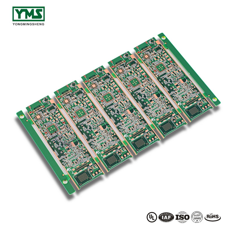
The 1 step HDI PCB is relatively simple and well controlled.
The 2 step HDI PCB is complicated due to alignment, punch and copper problems.
There are various 2 step HDI PCB designs.
One is the need for the staggered positions of the stages in the interlayer connection to connect the next layer via a wire, which is equivalent to a double 1 step HDI PCB.
The second is the overlap of two 1 step holes. Therefore, the 2 step PCB is implemented by superposition method, and the processing is similar to the 1 step, but there are many technical points that need special control.
The third is to rush directly from the outer layer to the third (or n-2) layer, a process that is quite different from the previous one and more difficult to drill.
Such as:
The 1 and 2 steps of the 6layer require laser drilling, or HDI boards.
The 6-layer 1 step HDI PCB refers to blind hole: 1-2, 2-5, 5-6. That is to say, 1-2-5-6 need laser drilling.
The 6-layer 2 step HDI board refers to blind hole: 1-2, 2-3, 3-4, 4-5, 5-6. It requires two laser drills.
First drill a 3-4 burrow, then layer 2-5,
Then drill 2-3 4-5 laser holes for the first time, then drill the second 1-6 layers.
Then drill 1-2-5- the second time is 6 laser holes.
It can be seen that the second-order HDI board has been laminated twice and laser drilled twice.
Circuit board laminating time:
1 step PCB: one lamination is sufficient, just like the most common PCB.
2 step PCB: coated twice. Take the eight-layer circuit board with blind/embedded hole as an example. Firstly, it is laminated 2-7. Firstly, the elaborately made blind/embedded hole is made.
3 step PCB: the process is much more complicated. First layer 3-6, then layer 2 and layer 7, and finally layer 1 and layer 8. It takes 3 laminating times, so most PCB manufacturers cannot make it.
Post time: Sep-25-2019

