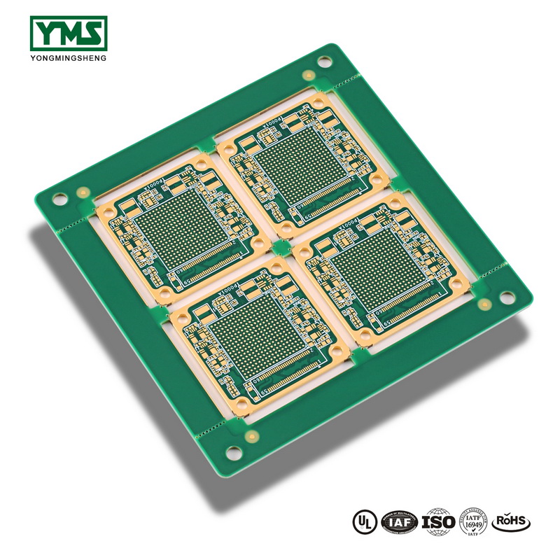
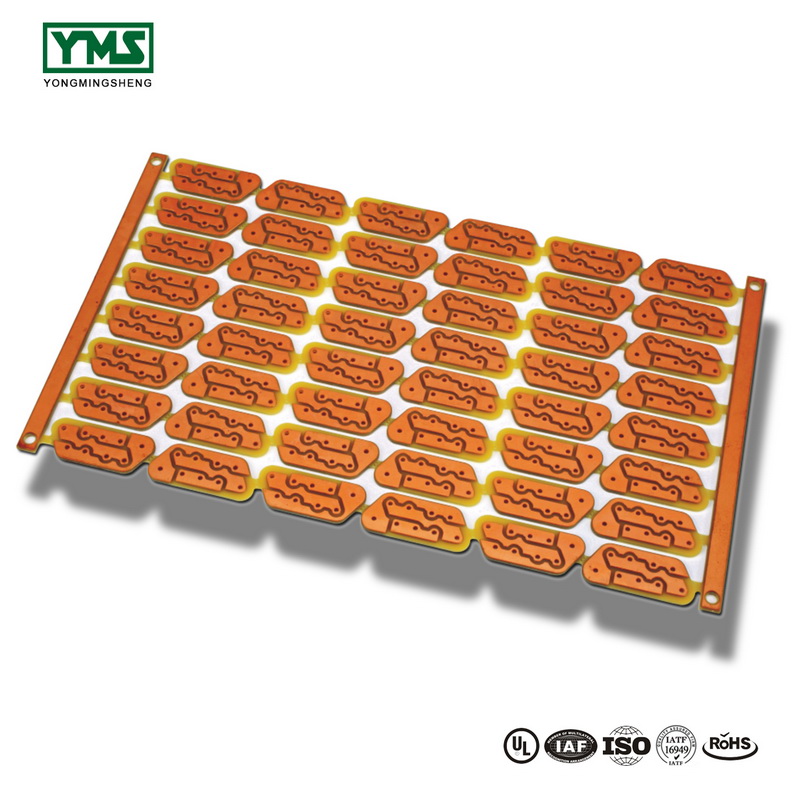
Heavy copper board can be divided into single-layer board, double-layer board, and multi-layer board according to the structure, the following small series of circuit board factory to detail the perforation mechanism of heavy copper board, miscellaneous plug hole and other related knowledge.
Double-layer board, high-tech development, people need high performance, small size, many functions of electronic products, promote printed circuit board manufacturing to light, thin, short, small development, limited space, to achieve more functions, wiring density, aperture is smaller.
Between 1995 and 2007, the minimum pore diameter of mechanical drilling batch capacity decreased from 0.4mm to 0.2mm or even smaller. The size of the metallized hole is getting smaller and smaller. The quality of the metallized holes on which layer to layer interconnect depends directly on PCB reliability.
With the reduction of aperture, the original sundries that have no effect on the larger aperture, such as grinding brush debris, volcanic ash, once remaining in the pore, will make the chemical copper sink, electroplating copper lose function, there is no copper hole, become the fatal killer of hole metallization.
I. porous mechanism
The drill bit is drilled on copper-coated board first, and then through chemical copper sinking, electroplating copper to form plated through hole. Both of them play an important role in the metallization of holes.
1. Mechanism of chemical copper precipitation:
In the manufacturing process of double-layer and multilayer PCB, the non-conductive bare holes need to be metallized, that is, the implementation of chemical copper deposition to make them become conductors.
Chemical copper solution is a catalytic oxidation/reduction reaction system. Under the catalysis of Ag, Pb, Au, Cu and other metal particles, copper was deposited.
2. Mechanism of copper plating:
Electroplating is defined as using a power source to push positively charged metal ions into position on the conductor surface of the cathode to form a coating. Electroplating copper is an “oxidation/reduction” reaction in which the copper anode in the solution oxidizes the copper metal on its surface to form copper ions. On the other hand, a reduction reaction occurs at the cathode and copper ions are deposited into copper metal. Both potions exchange, chemical effect to achieve the purpose of drilling, exchange effect directly affects the quality of drilling.
A copper layer shall be laid on the copper layer after the copper is formed in the inter-layer conduction hole channel to complete the inter-layer circuit conduction. Firstly, the hair on the hole was cleaned by heavy brushing and high-pressure washing, and then the rubber residue on the copper surface of the hole wall was removed by potassium permanganate solution.
The cleaned hole wall was soaked and attached with tin palladium colloid layer, which was then reduced to metal palladium. The circuit board was immersed in the chemical copper solution, and the copper ions in the solution were reduced and deposited on the pore wall by the catalysis of palladium metal, forming the through-hole circuit. Then the copper layer in the conducting hole is thickened by copper sulfate bath electroplating to a thickness sufficient to resist the subsequent processing and use of the dynamic impact of the environment.
II: sundry plug hole
In the long-term production control process, we found that when the aperture reaches 0.15-0.3mm, the proportion of the plug hole increases by 30%.
In check for a long time, we found that when drilling, residual impurities in hole here is the main cause of drilling plug hole: when a plug hole, due to the smaller aperture, high pressure water washing, chemical cleaning before sink copper is difficult to remove the inside of the hole sundry, Chinese medicine chemistry sink copper process water exchange in the hole, make chemical sink copper.
When drilling, the proper nozzle and backing board are selected according to the thickness of laminations to keep the base board clean, and the backing plate is not used repeatedly. The effective dust collection effect (independent dust control system is adopted) is the factor that must be considered to solve the plug hole.
III: draw circuit diagram
1. There are a variety of special PCB drawing software, such as Protel, etc., which can draw multi-layer (including double-layer) circuit board diagram, the multi-layer is aligned in position, and there are through holes to connect the lines between the layers, so as to realize cross wiring and facilitate typesetting. After typesetting can be handed over to professional manufacturers into a specific circuit board.
2. The double-layer board in turn draw circuit schematic diagram, can be divided into two steps.
Step 1: first draw the symbols of main components such as IC on the paper according to the position of the circuit board, connect the feet and the peripheral components properly and draw them to complete the sketch.
Step 2: analyze the principle and arrange the circuit diagram according to the conventional drawing method. Also, with the help of circuit schematic diagram software, connect the components after arranging, and then use its automatic typesetting function for sorting.
To accurately align the lines on both sides of the double panel, two tips of tweezers can be used for positioning, flashlight light transmission, multimeter measurement, etc., to determine the connection and direction of welding spots and lines, and if necessary, remove the components to observe the direction of the lines below.
Yongmingsheng technology co., LTD. is a high-tech company integrating circuit board development, design, proofing, production (processing), testing, production and sales.
The main products are: double-layer PCB, flexible Board, metal core PCB, reasonable price;
Since the establishment of the company, from the original professional circuit board processing, to expand the production of flexible circuit board, rigid circuit board, etc. We have been making progress, we have been committed to become a high quality PCB manufacturer and service provider.
Post time: Sep-12-2019


