What are the characteristics of double layer pcb board and multi-layer circuit board and how to distinguish them?Let’s follow the pcb board suppliers to understand:
Double layer pcb board
Double-sided Boards have wiring on both sides.But to use both sides of the wire, there must be a proper electrical connection between the two sides.This “bridge” between circuits is called a guide hole (VIA).A guide hole is a small hole in a PCB, filled or coated with metal, that can be connected to a wire on both sides.Because double panels have twice the area of a single panel, and because the wiring can be interlocked (which can be wound around the other side), it is better suited for more complex circuits than a single panel.
Technically double panel is a kind of PCB circuit board is very important in, he is the purpose of the great, to see if a board PCB board double panel is simple, understanding of a single panel is completely believe friends can grasp, is an extension of the single panel, double panel means single panel line enough to go to the opposite, double panel, and there was important feature is the guide hole.A simple point is that double-sided line, both sides of the line!A deeply touched bracket is: double sided line board is double panel!Some friends will ask such as a board double-sided wire, but only one side has electronic parts, such a board after all is a double panel or a single panel?The answer is obvious, such a board is a double panel, just in the double panel board mounted on the parts.
Multilayer circuit boards are simple to distinguish
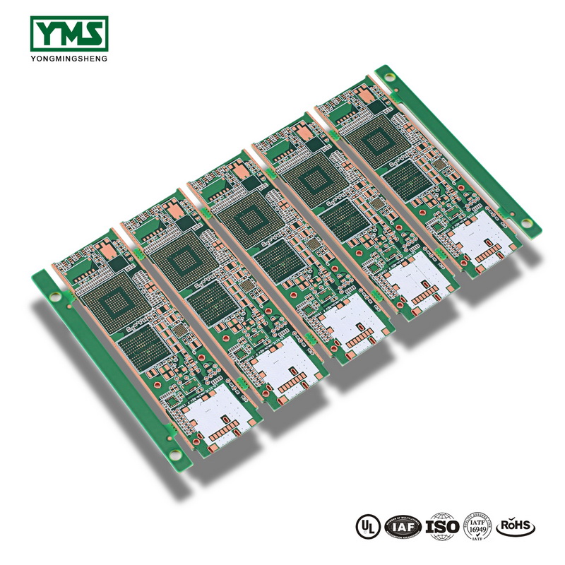
Circuit board according to decide how much of the wiring process difficulty and machining price, ordinary circuit board with single line and double line, commonly known as the single panel and double panel, high-end electronic products, however, because of product space design factors, in addition to the surface wiring, internal stack multilayer circuit, the process of production, made each layer after line, again through the optical device positioning, pressing, let the superposition of multi-layer circuit in a piece of circuit board.Commonly known as multilayer circuit board.Any circuit board greater than or equal to 2 layers can be called multi-layer circuit board.Multi-layer circuit board can be divided into multi-layer hard circuit board, multi-layer soft and hard circuit board, multi-layer soft and hard combined circuit board.
The birth of multilayer circuit board
The increased density of IC packages leads to a high concentration of interconnections, which necessitates the use of multiple substrates.Unforeseen design problems such as noise, stray capacitance, crosstalk appear in the layout of printed circuits.Therefore, PCB design must be aimed at minimizing the signal line length and avoiding parallel routes.Obviously, in a single panel, or even in a double panel, these requirements cannot be satisfactorily answered due to the limited number of crossings that can be implemented.In the case of a large number of interconnections and cross requirements, the board layer must be expanded to more than two layers to achieve a satisfactory performance.Therefore, the primary purpose of multi-layer circuit boards is to provide more freedom for complex and/or noise-sensitive electronic circuits to choose appropriate wiring paths.A multilayer circuit board has at least three conductive layers, two of which have an outer surface, and the remaining layer is synthesized in the insulation board.The electrical connection between them is usually made by plating through holes in the cross section of the circuit board.Multilayer printed circuit boards, like double panels, are generally plated through – orifice plates unless otherwise indicated.
Multilaminates are made by stacking two or more layers of circuits on top of each other, with reliable pre-set connections between them.Since drilling and electroplating are done before all the layers are rolled together, this technique violates the traditional manufacturing process from the start.The two innermost layers are made up of traditional double panels, while the outer layers are made up of separate single panels.Before being rolled, the inner plates will be drilled, electroplated through the holes, transferred graphically, developed and etched.The outer layer of the hole is the signal layer, which is plated through in such a way as to form a balanced copper ring at the inner edge of the hole.The layers are then rolled together to form a plurality of substrates, which can be interconnected by wave soldering.
The compaction may be done in a hydraulic press or in an overpressure chamber (autoclave).In the hydraulic press, the prepared material (for pressure stacks) is placed under cold or preheated pressure (the material for the high glass conversion temperature is placed at 170-180 ° C).The glass transition temperature is the temperature at which the amorphous region of a polymer (resin) or part of a crystalline polymer changes from a hard, rather brittle state to a viscous, rubbery state.
Multilaminates are put into use in specialized electronic equipment (computers, military equipment), especially in cases of weight and volume overload.However, this can only be achieved by increasing the cost of laminates in exchange for more space and less weight.In high-speed circuits, laminates are also very useful as they provide designers of printed circuit boards with more than two layers of boards for wiring and provide large areas of grounding and power.
The above is how to distinguish the double-sided circuit board and multi-layer circuit board, I hope you will like;We are circuit board manufacturers, welcome to inquire about ~
Post time: Oct-22-2020


