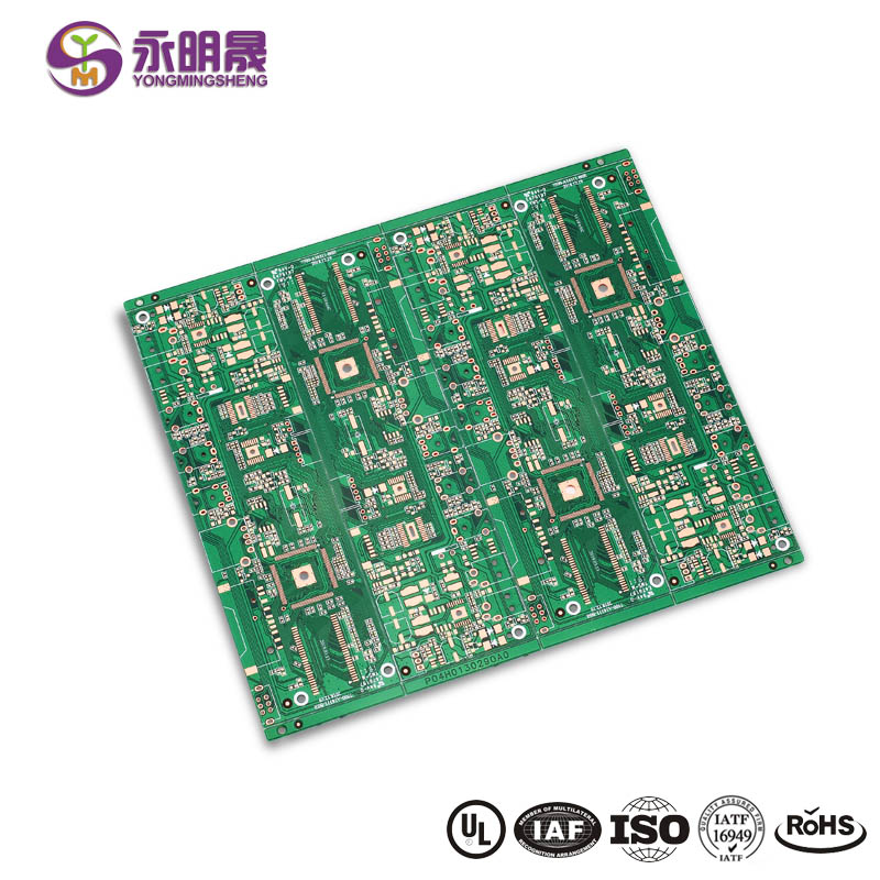
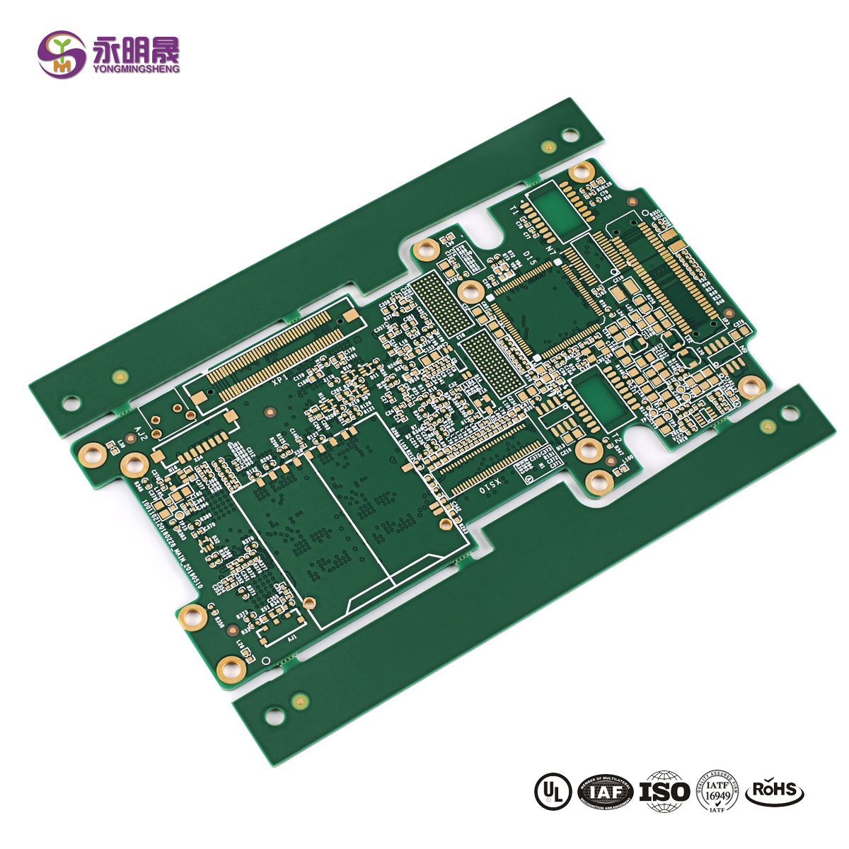
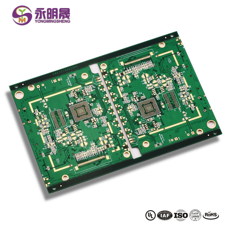
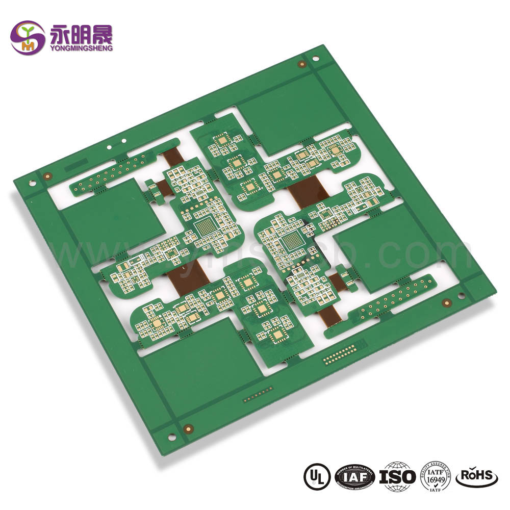
PCB can be classified by the number of circuit faces. Single-side board: only one side has wiring. Double-side board: wiring on both front and back. Multi-layer board: in addition to the surface wiring, there are several wiring layers inside.
The production process of all kinds of circuit boards is actually much the same, Cut Lamination, Drilling, PTH, Layer Image, Pattern Plate,etc.
But there are special processes for multi-layer boards, which is what we are going to focus on today.
1. Cut Lamination
Cut Lamination, also called Sheets Cutting, is the cutting of large base material to a suitable size. There are many kinds of base materials, fr-4 (glass fiberboard), aluminum substrate, copper substrate, ceramic plate, etc...There are many sizes and specifications of plates. For example, the most commonly used FR-4 has 37*49, 41*49, and 43*49(inch).
2. The inner processing
It’s a special process for multi-layer boards. Deal with the inner wiring first, then press the plates together.
①Inner Layer Drilling
According to the requirements, complete the inner holes, Blind/Buried holes.
②Pretreatment
Grind board, increase the roughness of the plate surface so that the binding force of the copper surface and the layer of photosensitive oil (or dry film) is strengthened.
③Roll or film
Apply light-sensitive oil or laminate photosensitive dry film to the surface.
④Exposure
Use an exposure machine to transfer the image of the inner film to a plate with a photosensitive surface.
⑤DES(Developing, Etching & Stripping)
Developing: remove the ink from the unexposed part to expose the copper surface.
Etching: etch copper exposed after development.
Stripping:de-film, wash and dry to remove residual ink, until exposing the required circuit.
⑥AOI
Check various quality phenomena, such as open circuit, short circuit, gap, etc.
⑦Lamination
Black Oxide Treatment: through a chemical reaction, the copper surface of the circuit forms an oxide film on the surface.
Layup: according to the laminating structure drawing, choose the correct PP and inner layer plate combination, and place copper foil in the outermost layer.
Lamination: By applying pressure and high temperature, PP is melted and re-solidified, so that the layers are combined as a whole. And then through cooling pressure, prevent deformation.
3. Drilling
According to the requirements, complete all other holes. PTH (plated through-hole): Via hole, IC hole. NPTH (Non-plated through-hole): Positioning holes, and tool holes for assembly parts.
4. Outer line processing
The general flow that all the remaining category boards have, we'll cover in a future article.
Read more news
Learn more about YMS products
Post time: Jun-24-2022


