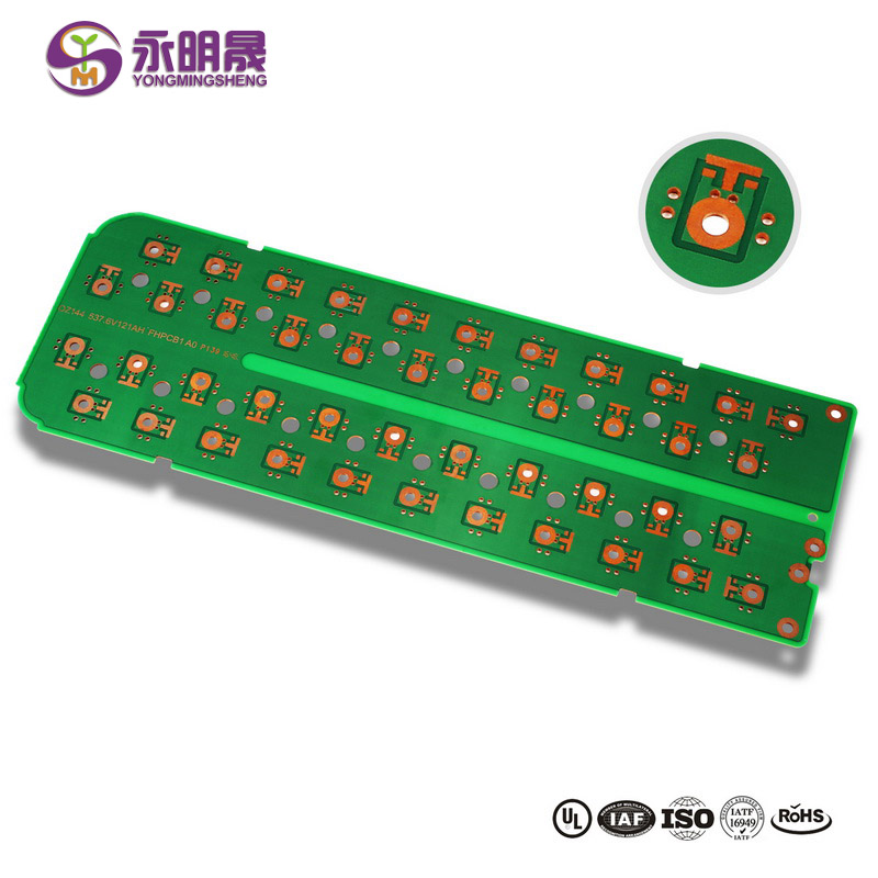
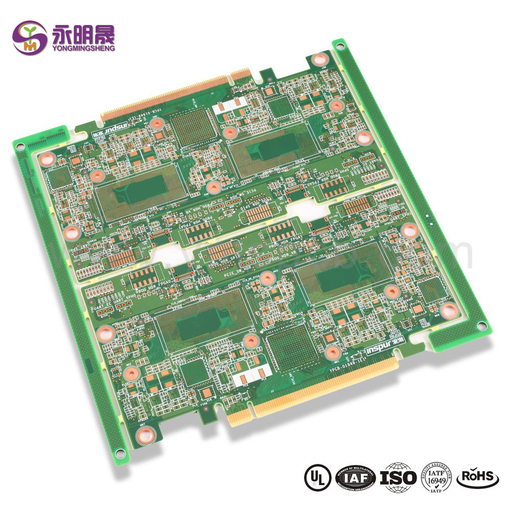
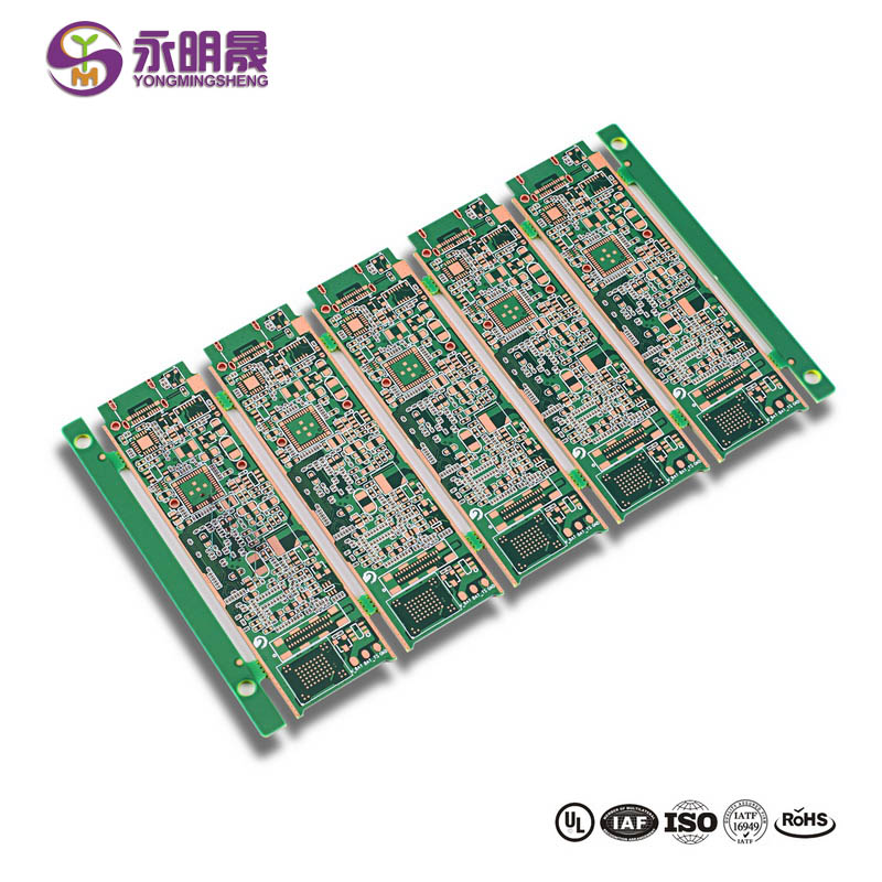
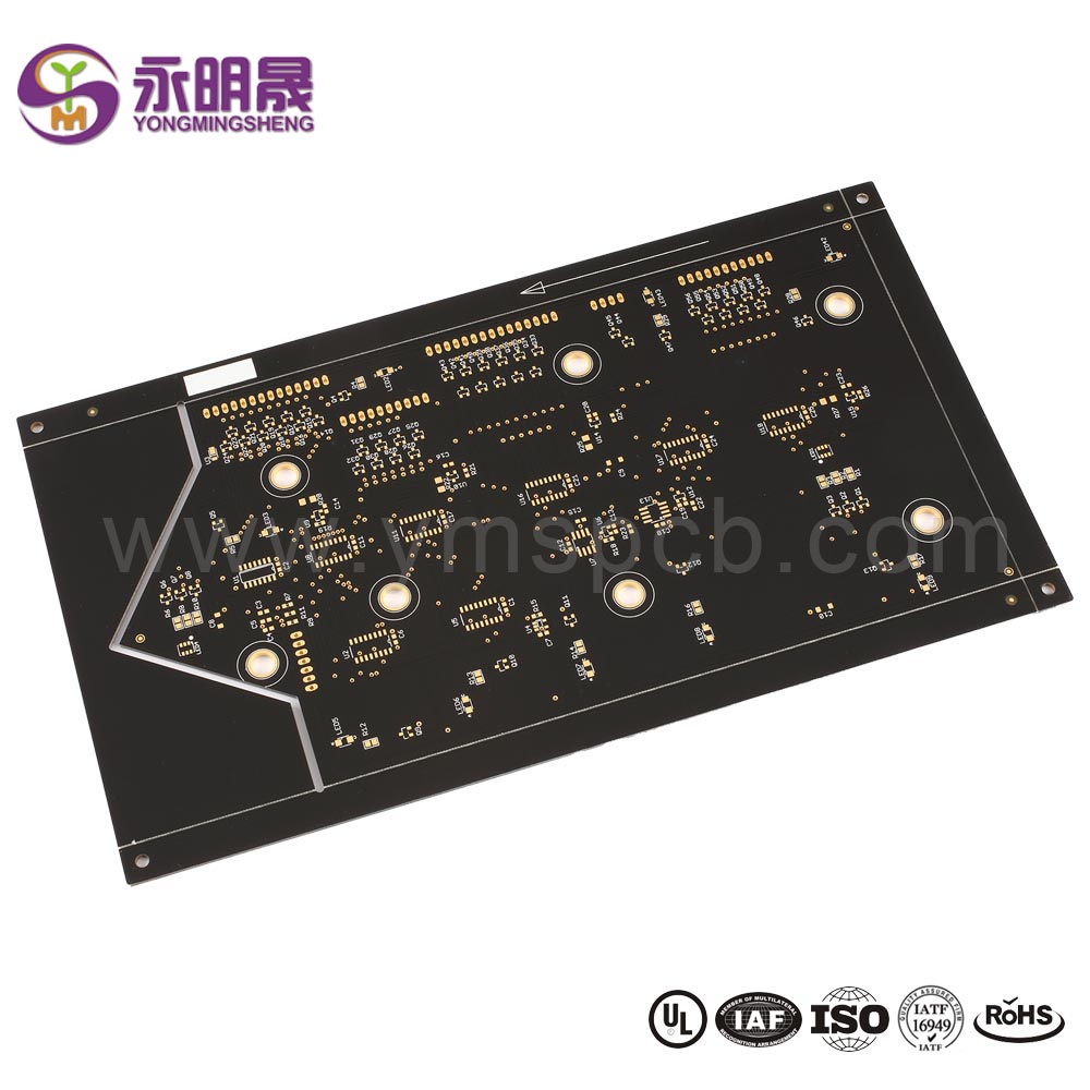
Ceramic PCBs are composed of a ceramic substrate, a connection layer, and a circuit layer. Unlike MCPCB, ceramic PCBs do not have an insulation layer, and manufacturing the circuit layer on the ceramic substrate is difficult. How are ceramic PCBs manufactured? Since the ceramic materials were used as PCB substrates, quite a few methods were developed to manufacture the circuit layer on a ceramic substrate. These methods are HTCC, DBC, thick film, LTCC, thin-film, and DPC.
HTCC
Pros: high structural strength; high thermal conductivity; good chemical stability; high wiring density;RoHS certified
Cons: poor circuit conductivity; high sintering temperatures; expensive cost
HTCC is an abbreviation of high-temperature co-fired ceramic. It is the earliest ceramic PCB manufacturing method. The ceramic materials for HTCC are alumina, mullite, or aluminum nitride.
Its manufacturing process is:
At 1300-1600℃, ceramic powder (without glass added) is sintered and dried to solidify. If the design requires through holes, holes are drilled on the substrate board.
At the same high temperatures, high-melting-temperature metal is melted as a metal paste. The metal can be tungsten, molybdenum, molybdenum, manganese, and so on. The metal can be tungsten, molybdenum, molybdenum, and manganese. The metal paste is printed according to the design to form a circuit layer on the circuit substrate.
Next, 4%-8% sintering aid is added.
If the PCB is multilayer, layers are laminated.
Then at 1500-1600℃, the whole combination is sintered to form the ceramic circuit boards.
Finally, the solder mask is added to protect the circuit layer.
Thin Film Ceramic PCB Manufacturing
Pros: lower manufacturing temperature; fine circuit; good surface flatness
Cons: expensive manufacturing equipment; can't manufacture three-dimensional circuits
The copper layer on the thin film ceramic PCBs has thicknesses smaller than 1mm. The main ceramic materials for thin-film ceramic PCBs are alumina and aluminum nitride. Its manufacturing process is:
The ceramic substrate is cleaned first.
In vacuum conditions, moisture on the ceramic substrate is thermally evaporated.
Next, a copper layer is formed on the ceramic substrate surface by magnetron sputtering.
The circuit image is formed on the copper layer by yellow-light photoresist technology.
Then the excessive copper is removed by etching.
Finally, the solder mask is added to protect the circuit.
Summary: the thin film ceramic PCB manufacturing is finished in vacuum condition. The yellow light lithography technology allows more precision to the circuit. However, thin-film manufacturing has a limit to copper thickness. Thin-film ceramic PCBs are suitable for high-precision packaging and devices in a smaller size.
DPC
Pros: no limit to the ceramic type and thickness; fine circuit; lower manufacturing temperature; good surface flatness
Cons: expensive manufacturing equipment
DPC is the abbreviation of direct plated copper. It develops from the thin film ceramic manufacturing method and improves by adding the copper thickness through plating. Its manufacturing process is:
The same manufacturing process of the thin-film manufacturing until the circuit image is printed on the copper film.
The circuit copper thickness is added by plating.
The copper film is removed.
Finally, the solder mask is added to protect the circuit.
Conclusion
This article lists the common ceramic PCB manufacturing methods. It introduces the ceramic PCB manufacturing processes and gives a brief analysis of the methods. If engineers/solutions companies/institutes want to have ceramic PCBs manufactured and assembled, YMSPCB will bring 100% satisfying results to them.
Video
Learn more about YMS products
Post time: Feb-18-2022


Board5.jpg)