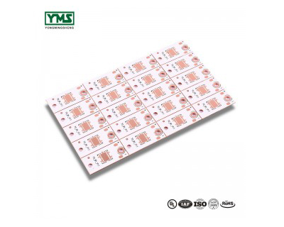
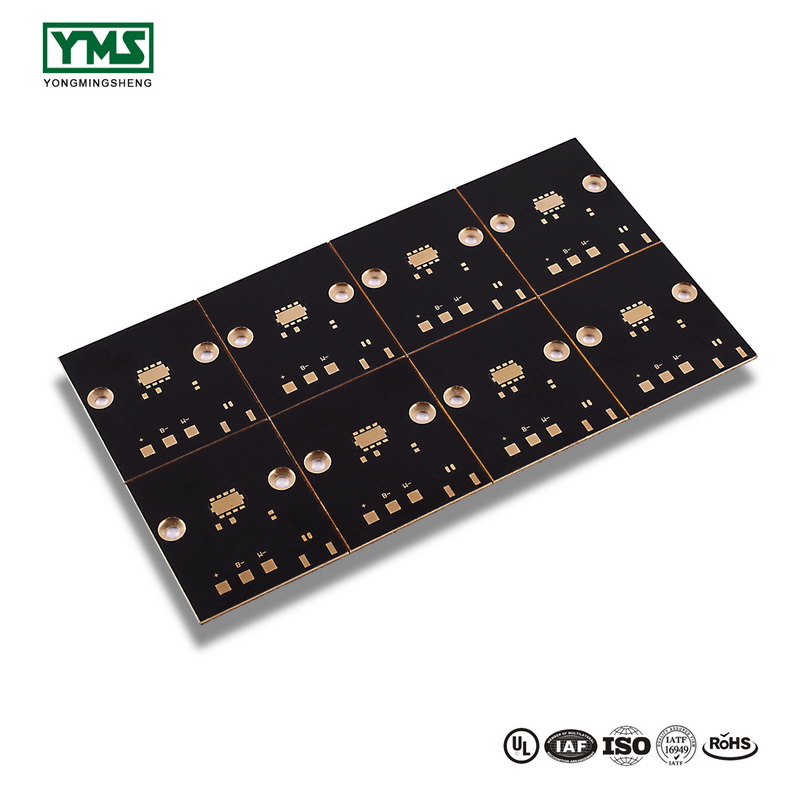
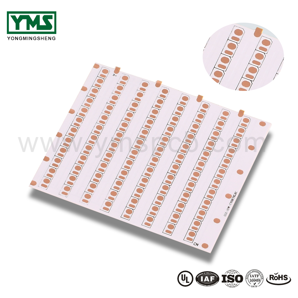
First appeared in 1950 single sided pcb board, single-sided PCB material use paper phenolic backing board, double-sided circuit board is simple to understand both sides have wiring, thus better distinction, panel is more greater than 2 layers, wiring how much difficulty and price, specific content please follow China PCB manufacturers to understand:
History of single-sided circuit board:
Single-sided printed circuit board is a product developed in the United States with the appearance of transistors in the early 1950s. At that time, direct etching of copper foil was the main production method.
In 1953-1955, Japan used imported copper foil to make paper phenolic copper foil substrate for the first time, and it was widely used in radio.
In 1956, after the emergence of professional manufacturers of circuit boards in Japan, the manufacturing technology of single panel immediately advanced rapidly.
In terms of materials, at the early stage, paper phenolic copper foil substrate was the main material. However, due to the low electrical insulation, poor welding heat resistance, distortion and other factors of phenolic material at that time, materials such as paper ring gas resin and glass fiber epoxy resin were gradually developed. At present, the single panel required by consumer electronic machines almost adopts paper phenolic resin substrate.
Features of single-sided circuit board:
The single panel is on the most basic PCB, with the parts concentrated on one side and the wires on the other.Since wires appear only on one side, we call this TYPE of PCB single-sided.Only early circuits used such boards because of the strict limitations of single panels in the design circuit (because only one side of the circuit could not be crossed and had to be wound around a separate path);
The wiring diagram of single panel is dominated by Screen Printing, which means blocking agent is printed on the copper surface, etched to prevent solder Printing marks, and finally punching processing is used to complete the parts’ guide holes and shapes.In addition, for some products produced in small quantities and in a variety of ways, a photographic process in which a pattern is formed by a photosensitizer is used.
The above is about the history of the circuit board and characteristics of the introduction, I hope to have some help for you ~!We are a pcb board manufacturer, welcome your consultation ~
Post time: Oct-22-2020


