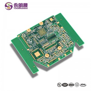
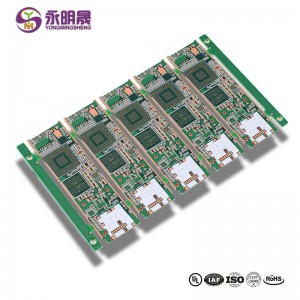
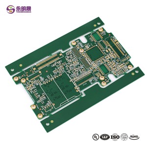
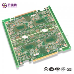
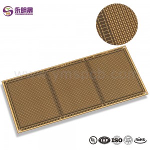
LED display screen pcb HDI laser via in PAD copper plated shut| YMSPCB
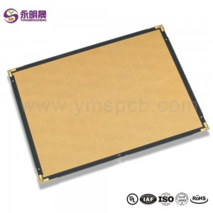
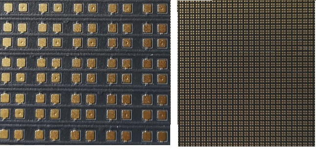
What is LED display screen printed circuit board:
LED display, also known as LED screen, LED video wall, LED panel or LED signage, has gradually replaced traditional billboards, light boxes and so on with its unique advantages. LED display advertising has become a new force in the media industry.
Traditional ads can only display images, but the LED display / LED display / LED screen can be a perfect combination of text, pictures, video and sound, and you can change the presentation as needed.
Which can be flexibly played through the display player software settings, and has high resolution, high brightness and full color!
The LED display advertising screen can easily attract the attention of pedestrians, and is easy to remember, which can produce greater advertising effects.
LED displays are now widely used in media advertising, transportation, security, real estate and stage performance backgrounds.
The LED display is beautiful and not easily damaged, and has a long service life, which saves a lot of unnecessary costs and expenses.
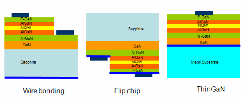
Schematic diagrams of wire bonding flip chip and ThinGaN LEDs
YMS LED display screen pcb manufacturing capabilities:
| YMS LED display screen pcb manufacturing capabilities overview | |
| Feature | capabilities |
| Layer Count | 1-60L |
| Available LED display screen pcb Technology | 1+N+1 |
| 2+N+2 | |
| 3+N+3 | |
| 4+N+4 | |
| 5+N+5 | |
| Any layer | |
| Thickness | 0.3mm-6mm |
| Minimum line Width and Space | 0.05mm/0.05mm(2mil/2mil) |
| Light Emitting Diode PITCH | P0.47mm;P0.58mm;P0.70mm;P0.77mm;P0.925mm;P1.0mm;etc. |
| Min laser Drilled Size | 0.075mm(3nil) |
| Min mechanical Drilled Size | 0.15mm(6mil) |
| Aspect Ratio for laser hole | 0.9:1 |
| Aspect Ratio for through hole | 16:1 |
| Surface Finish | HASL, Lead free HASL,ENIG,Immersion Tin, OSP, Immersion Silver, Gold Finger, Electroplating Hard Gold, Selective OSP,ENEPIG.etc. |
| Via Fill Option | The via is plated and filled with either conductive or non-conductive epoxy then capped and plated over |
| Copper filled, silver filled | |
| Laser via copper plated shut | |
| Registration | ±4mil |
| Solder Mask | Green, Red, Yellow, Blue, White, Black, Purple, Matte Black, Matte green.etc. |
- It is beneficial to use LED PCB as it helps electronics get thinner and smaller. Its numerous applications include but not limited to:
-
1. Telecom LED PCB
Telecommunication devices use LED displays and indicators. The LEDs offer decreased weight, improved durability, and enhanced heat transfer. So, they are much useful in the telecom sector applications such as high-frequency amplifiers and filtering appliances.
-
2. Automotive LED PCB
They can be found in car indicators, brake lights, headlights, and other devices. Longevity, durability, and low prices are the reason that LED PCBs aluminum PCB are common in the automotive industry.
-
3. Computer LED PCB
They are also becoming common in computer equipment as indicators and displays. The LED PCB board is an ideal solution for the heat-sensitive computer machinery.
-
4. Medical LED PCB
In medical examinations and surgeries, high-powered LED lighting tools are used. They ensure the proper function of the medical equipment regardless of the number of patients in the medical office.
-
5. Other LED PCB
Other application fields of LED PCB board are airport runway lights, street lighting, photovoltaic (solar) lightening, lanterns and flashlights, highway tunnel lightening, highway growth plant, signal, and traffic lighting.
LED PCBs are best for consumer devices, some marine and aviation applications, flashlight and other camping accessories in lower-light environments, elevator lighting, power converters, decorative and concealed lights, and many more
Learn more about YMS products


