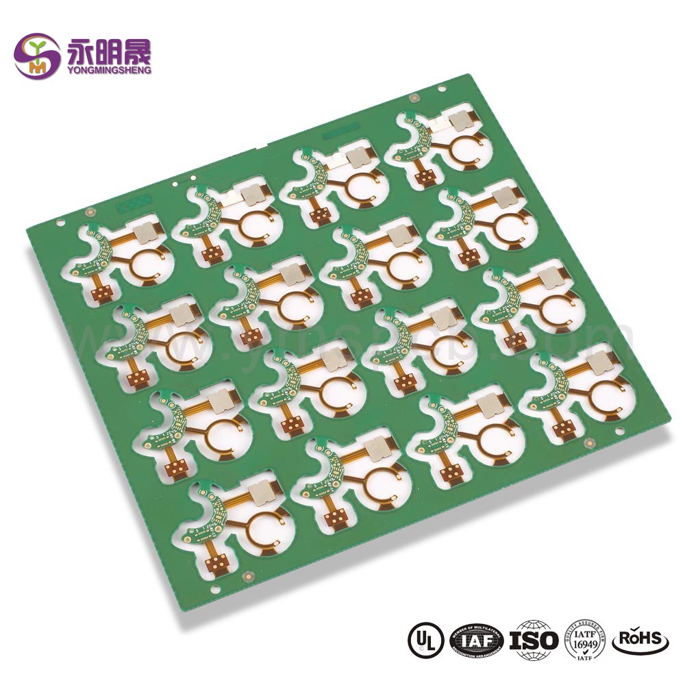
Double sided pcb Normal pcb Lead free HASL Counterbore Manufacturer | YMS PCB
HAL(Lead Free), the full name is Hot Air leveling with Lead Free. Compared with HASL, the main difference for HAL(Lead Free) is the element of material which do not contain Lead(Pb), so it’s RoHS Compliant and it’s much more popular and widely used in PCB製造.
HAL(Lead Free) requires higher run temperatures for lead free solder and longer contact time, the production cost for HAL(Lead Free) is slightly higher than HASL(Tin/Lead).
The manufacturing process of HAL(Lead Free) is similar to HASL(Tin/Lead), the circuit boards will be submersed in molten solder(Lead Free). This solder will cover all the exposed copper surfaces. Upon retraction from the solder, high pressure hot air is blown over the surface through air knives, this levels the solder deposit and removes the excess solder from the surface of printed circuit boards.
プリント基板の紹介
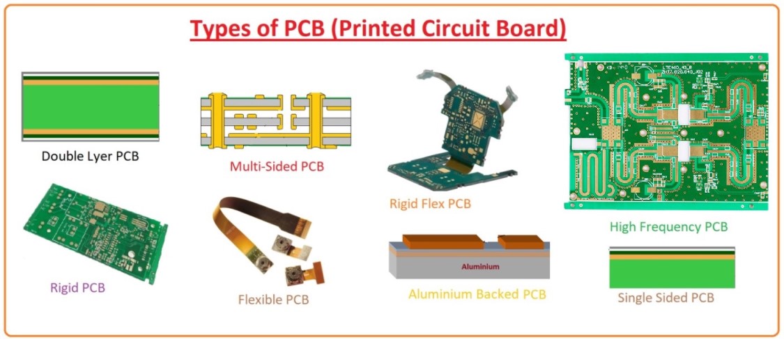
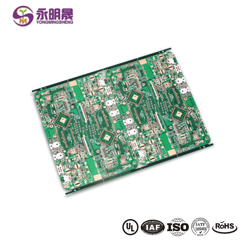
通常のプリント回路基板: Most PCBs for simple electronics are simple and composed of only a single layer. More sophisticated hardware such as computer graphics cards or motherboards can have 2 or multiple layers, sometimes up to twelve.
A printed circuit board (PCB) mechanically supports and electrically connects electrical or electronic components using conductive tracks, pads and other features etched from one or more sheet layers of copper laminated onto and/or between sheet layers of a non-conductive substrate. Components are generally soldered onto the PCB to both electrically connect and mechanically fasten them to it.PCBs can be single-sided (one copper layer), double-sided (two copper layers on both sides of one substrate layer), or multi-layer (outer and inner layers of copper, alternating with layers of substrate). Multi-layer PCBs allow for much higher component density, because circuit traces on the inner layers would otherwise take up surface space between components. The rise in popularity of multilayer PCBs with more than two, and especially with more than four, copper planes was concurrent with the adoption of surface mount technology.
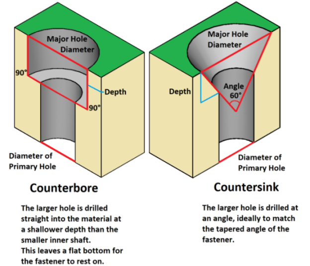
What is the difference between a Countersink and a Counterbore?
YMS通常のPCB製造機能:
| YMS通常のPCB製造機能の概要 | ||
| 特徴 | 機能 | |
| レイヤー数 | 1-60L | |
| 利用可能な通常のPCBテクノロジー | アスペクト比16:1のスルーホール | |
| 埋葬され、盲目 | ||
| ハイブリッド | RO4350BやFR4ミックスなどの高周波素材。 | |
| M7NEやFR4Mixなどの高速素材。 | ||
| 材料 | CEM- | CEM-1; CEM-2; CEM-4; CEM-5.etc |
| FR4 | EM827、370HR、S1000-2、IT180A、IT158、S1000 / S1155、R1566W、EM285、TU862HF、NP170Gなど。 | |
| 高速 | Megtron6、Megtron4、Megtron7、TU872SLK、FR408HR、N4000-13シリーズ、MW4000、MW2000、TU933など。 | |
| 高周波 | Ro3003、Ro3006、Ro4350B、Ro4360G2、Ro4835、CLTE、Genclad、RF35、FastRise27など。 | |
| その他 | ポリイミド、Tk、LCP、BT、Cプライ、Fradflex、オメガ、ZBC2000、PEEK、PTFE、セラミックベースなど。 | |
| 厚さ | 0.3mm-8mm | |
| 最大銅厚 | 10OZ | |
| 最小線幅とスペース | 0.05mm / 0.05mm(2mil / 2mil) | |
| BGAピッチ | 0.35mm | |
| 最小機械ドリルサイズ | 0.15mm(6mil) | |
| スルーホールのアスペクト比 | 16:1 | |
| 表面仕上げ | HASL、鉛フリーHASL、ENIG、イマージョンスズ、OSP、イマージョンシルバー、ゴールドフィンガー、電気めっきハードゴールド、選択的OSP、ENEPIGなど。 | |
| 塗りつぶしオプション経由 | ビアは、導電性または非導電性エポキシのいずれかでメッキおよび充填されてから、キャップおよびメッキが施されます(VIPPO) | |
| 銅充填、銀充填 | ||
| 登録 | ±4mil | |
| 戦士の表情 | 緑、赤、黄、青、白、黒、紫、マットブラック、マットグリーンなど。 | |
あなたは好きかもしれません:
1、Summary of matters needing attention in circuit board welding
5. 高周波PCB設計とは


