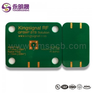
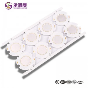
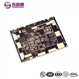
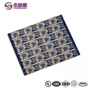
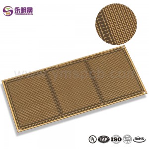
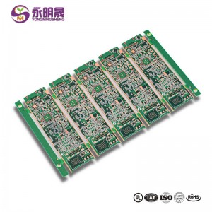
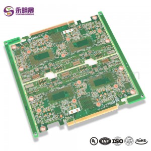
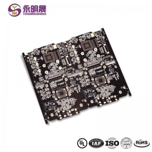
Ikanam ngosi ihuenyo pcb HDI laser via na PAD ọla kọpa plated mechie | YMSPCB
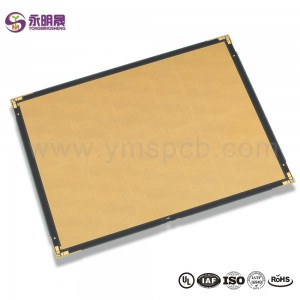
Gịnị bụ ikanam ngosi ihuenyo ndị e biri ebi circuit iba:
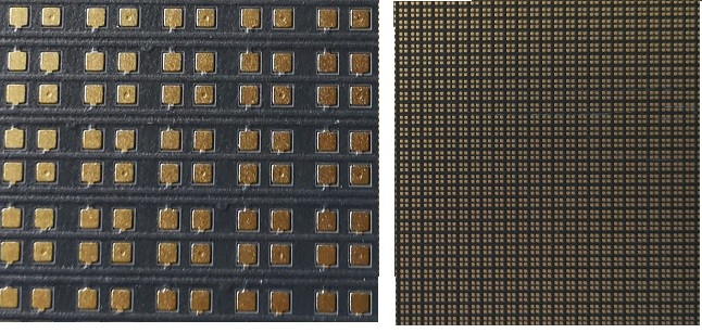
Ikanam ngosi, makwaara dị ka Ikanam ihuenyo, Ikanam video mgbidi, Ikanam panel ma ọ bụ Ikanam signage, ji nwayọọ nwayọọ dochie ọdịnala ọdịnala, igbe ọkụ na na na ya pụrụ iche uru. Ikanam ngosi mgbasa ozi aghọwo ike ọhụrụ na ụlọ ọrụ mgbasa ozi.
Omenala mgbasa ozi nwere ike igosipụta onyogho, mana ngosi Ikanam / Ikanam ngosi / Ikanam ihuenyo nwere ike ịbụ ngwakọta zuru oke nke ederede, eserese, vidiyo na ụda, ị nwere ike ịgbanwe ngosi dịka ọ dị mkpa.
Kedu nke enwere ike igwu egwu site na ntọala ngwanrọ ngosi ihe ngosi, ma nwee mkpebi dị elu, nchapụta dị elu na agba zuru oke!
Ikanam ngosi mgbasa ozi mgbasa ozi nwere ike ịdọrọ uche nke ndị na-agafe agafe, ọ dịkwa mfe icheta, nke nwere ike mepụta mmetụta mgbasa ozi ka ukwuu.
Ikanam ngosipụta bụ ugbu a n'ọtụtụ ebe na media mgbasa ozi, njem, nche, ezigbo ala na ụlọ na ogbo arụmọrụ nsio.
Ihe ngosi Ikanam mara mma ma ọ naghị adị mfe mmebi, ma nwee ogologo ndụ ọrụ, nke na-azọpụta ọtụtụ ụgwọ na mmefu na-enweghị isi.
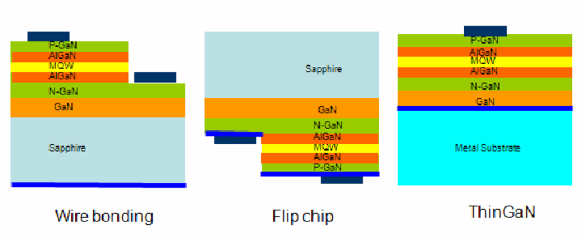
Schematic diagrams of wire bonding flip chip and ThinGaN LEDs
YMS Ikanam ngosi ihuenyo PCB n'ichepụta ike:
| YMS Ikanam ngosi ihuenyo pcb n'ichepụta ike nnyocha | |
| Njirimara | ikike |
| Layer agụ | 1-60L |
| Dị Ikanam ngosi ihuenyo PCB Technology | 1 + N + 1 |
| 2 + N + 2 | |
| 3 + N + 3 | |
| 4 + N + 4 | |
| 5 + N + 5 | |
| Ọ bụla oyi akwa | |
| Ọkpụrụkpụ | 0.3mm-6mm |
| Opekempe akara Obosara na Ohere | 0.05mm / 0.05mm (2mil / 2mil) |
| Light Emitting Diode PITCH | P0.47mm; P0.58mm; P0.70mm; P0.77mm; P0.925mm; P1.0mm; wdg. |
| Min laser gbapuru Size | 0.075mm (3nil) |
| Min n'ibu gbapuru Size | 0.15mm (6mil) |
| Akụkụ ruru maka laser onu | 0.9: 1 |
| Akụkụ Ratio maka site na oghere | 16: 1 |
| Elu rụchaa | HASL, Duru free HASL, ENIG, Imikpu Tin, OSP, ọlaọcha imikpu, mkpịsị aka mkpịsị aka, Ntinye ọla edo siri ike, ịhọrọ OSP , ENEPIG.etc. |
| Via Dejupụta Nhọrọ | The via na-plated ma jupụta ma conductive ma ọ bụ ndị na-abụghị conductive epoxy ahụ capped na plated |
| Ọla kọpa jupụtara, ọlaọcha jupụtara | |
| Laser site na ọla kọpa plated mechie | |
| Ndebanye aha | ± 4mil |
| Nkpuchi Solder | Green, Red, Yellow, Blue, White, Nwa, Purple, Matte Black, Matte green. Wdg. |
- It is beneficial to use LED PCB as it helps electronics get thinner and smaller. Its numerous applications include but not limited to:
-
1. Telecom LED PCB
Telecommunication devices use LED displays and indicators. The LEDs offer decreased weight, improved durability, and enhanced heat transfer. So, they are much useful in the telecom sector applications such as high-frequency amplifiers and filtering appliances.
-
2. Automotive LED PCB
They can be found in car indicators, brake lights, headlights, and other devices. Longevity, durability, and low prices are the reason that LED PCBs aluminum PCB are common in the automotive industry.
-
3. Computer LED PCB
They are also becoming common in computer equipment as indicators and displays. The LED PCB board is an ideal solution for the heat-sensitive computer machinery.
-
4. Medical LED PCB
In medical examinations and surgeries, high-powered LED lighting tools are used. They ensure the proper function of the medical equipment regardless of the number of patients in the medical office.
-
5. Other LED PCB
Other application fields of LED PCB board are airport runway lights, street lighting, photovoltaic (solar) lightening, lanterns and flashlights, highway tunnel lightening, highway growth plant, signal, and traffic lighting.
LED PCBs are best for consumer devices, some marine and aviation applications, flashlight and other camping accessories in lower-light environments, elevator lighting, power converters, decorative and concealed lights, and many more
Mụtakwuo maka ngwaahịa YMS


