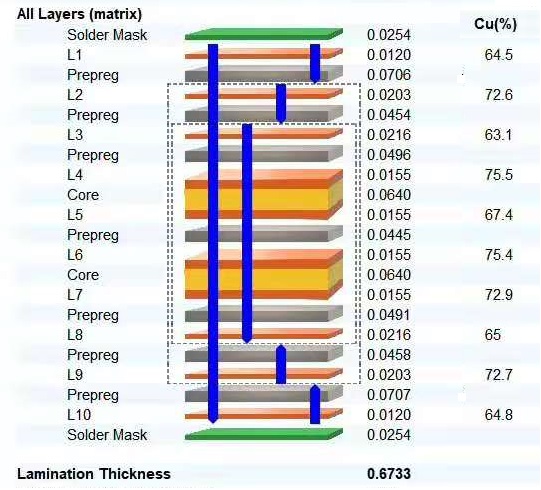
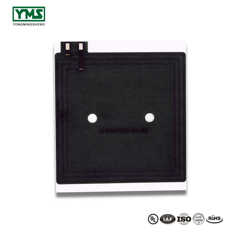
Hot Selling for Hcpv Solar Thermal Ceramic Substrate - High Density Interconnect PCB 10Layer 2 Step HDI Board| YMS PCB – Yongmingsheng
Hot Selling for Hcpv Solar Thermal Ceramic Substrate - High Density Interconnect PCB 10Layer 2 Step HDI Board| YMS PCB – Yongmingsheng Detail:
What is HDI PCB
HDI PCB: High density interconnect PCB, are a way of making more room on your printed circuit board to make them more efficient and allow for faster transmission. It’s relatively easy for most enterprising companies that are using printed circuit boards to see how this can benefit them.
Advantages of HDI PCB
The most common reason for using HDI technology is a significant increase in packaging density. The space obtained by finer track structures is available for components. Besides, overall space requirements are reduced will result in smaller board sizes and fewer layers.
Usually FPGA or BGA are available with 1mm or less spacing. HDI technology makes routing and connection easy, especially when routing between pins.
YMS HDI PCB manufacturing capabilities:
| YMS HDI PCB manufacturing capabilities overview | |
| Feature | capabilities |
| Layer Count | 4-60L |
| Available HDI PCB Technology | 1+N+1 |
| 2+N+2 | |
| 3+N+3 | |
| 4+N+4 | |
| 5+N+5 | |
| Any layer | |
| Thickness | 0.3mm-6mm |
| Minimum line Width and Space | 0.05mm/0.05mm(2mil/2mil) |
| BGA PITCH | 0.35mm |
| Min laser Drilled Size | 0.075mm(3nil) |
| Min mechanical Drilled Size | 0.15mm(6mil) |
| Aspect Ratio for laser hole | 0.9:1 |
| Aspect Ratio for through hole | 16:1 |
| Surface Finish | HASL, Lead free HASL,ENIG,Immersion Tin, OSP, Immersion Silver, Gold Finger, Electroplating Hard Gold, Selective OSP,ENEPIG.etc. |
| Via Fill Option | The via is plated and filled with either conductive or non-conductive epoxy then capped and plated over |
| Copper filled, silver filled | |
| Laser via copper plated shut | |
| Registration | ±4mil |
| Solder Mask | Green, Red, Yellow, Blue, White, Black, Purple, Matte Black, Matte green.etc. |
You May Like:
2、HDI PCB market supply and demand analysis and circuit advantages
3、How to define the order of HDI board
Product detail pictures:

Related Product Guide:
PCB & PCBA Market Outlook by Responsible Drivers, Restraints, Demand & Forecasts by 2024 | 1.2m 2layer Led Pcb
High-Density Interconnect (HDI) PCB Market Expected to Expand at a Steady CAGR through 2026 | Rigid-Flexible Pcb
Our enterprise insists all along the standard policy of "product high-quality is base of business survival; client satisfaction could be the staring point and ending of an business; persistent improvement is eternal pursuit of staff" as well as consistent purpose of "reputation first, client first" for Hot Selling for Hcpv Solar Thermal Ceramic Substrate - High Density Interconnect PCB 10Layer 2 Step HDI Board| YMS PCB – Yongmingsheng , The product will supply to all over the world, such as: Toronto, Bangladesh, Slovakia, The president and all the company members would like to provide professional products and services for customers and sincerely welcome and cooperate with all native and foreign customers for a bright future.
The after-sale warranty service is timely and thoughtful, encounter problems can be resolved very quickly, we feel reliable and secure.


