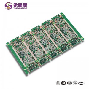
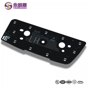
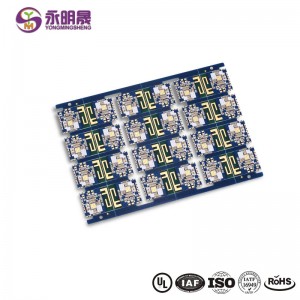
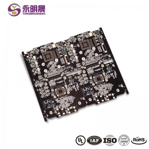
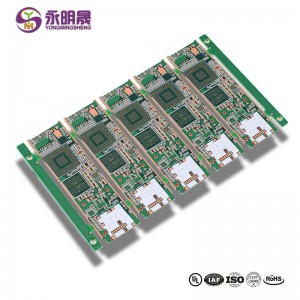
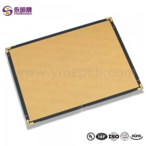
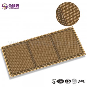
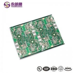
HDI PCB 12 Layer 2 Step HDI Board | YMS PCB
tsis
Khaubncaws sab nraud povtseg: 12
Base Material:FR4 High Tg EM827
Thickness : 1.2 ± 0.1mm
Min.Hole Size:0.15mm
Minimum Line Width/Space:0.075mm/0.075mm
Kev Tawm Tsam Tsawg Kom Nruab Nrab ntawm Txheej Txheej PTH thiab Kab : 0.2mm
Size:101mm×55mm
Nam piv: 8: 1
Deg kev kho mob: ENIG
Speciality: Laser via copper plated shut,VIPPO Technology,Blind Via and Buried Hole
Daim ntaub ntawv: Telecommunication
What is HDI PCBs?
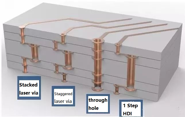
High density interconnect (HDI) PCBs represent one of the fastest-growing segments of the printed circuit board market. Because of its higher circuitry density, the HDI PCB design can incorporate finer lines and spaces, smaller vias and capture pads, and higher connection pad densities. A high-density PCB features blind and buried vias and often contains microvias that are .006 in diameter or even less.
1.Multi-step HDI enables cov kev twb kev txuas ntawm tej khaubncaws sab nraud povtseg;
2.Cross-txheej laser ua yuav txhim khu kev theem ntawm multi-step HDI;
3.The ua ke ntawm HDI thiab high-zaus cov ntaub ntawv, hlau-raws li laminates, FPC thiab lwm yam tshwj xeeb laminates thiab cov txheej txheem pab kom cov kev xav tau ntawm kev kub ceev thiab siab zaus, siab kub kev, los yog 3D los ua ke.
YMS HDI PCB tsim cov peev txheej:
| YMS HDI PCB kev tsim khoom muaj peev xwm txheej txheem cej luam | |
| Ntseg | muaj peev xwm |
| Txheej Txheej | 4-60L |
| Muaj HDI PCB Tshuab | 1 + N + 1 |
| 2 + N + 2 | |
| 3 + N + 3 | |
| 4 + N + 4 | |
| 5 + N + 5 | |
| Txhua txheej | |
| Thickness | 0.3mm-6mm |
| Yam tsawg kawg kab Dav thiab qhov chaw | 0.05mm / 0.05mm (2mil / 2mil) |
| BGA CHAW | 0.35 hli |
| Min laser Drilled Qhov loj me | 0.075mm (3nil) |
| Min mechanical Drilled Qhov Coob | 0.15 hli (6mil) |
| Aspect Piv rau laser lub qhov | 0.9: 1 |
| Saib tus ntsuas rau ntawm lub qhov | 16: 1 |
| Nto xaus | HASL, Lead dawb HASL, ENIG, Immersion Tin, OSP, Immersion Silver, Gold Finger, Electroplating Hard Kub, Xaiv OSP , ENEPIG.etc. |
| Ntawm Cov Kev Xaiv Sau | Qhov ntawm yog plated thiab muaj nrog cov conductive lossis tsis-conductive epoxy ces capped thiab plated dua |
| Tooj liab ntim, tau sau nyiaj | |
| Laser ntawm tooj liab plated kaw | |
| Sau npe | 4mil |
| Tus Neeg Muag Khoom Daim npog qhov ncauj | Ntsuab, Liab, Daj, Xiav, Dawb, Dub, Ntshav, Matte Dub, Matte green.etc. |
Koj tuaj yeem nyiam:
1, The application range and circuit advantage of HDI board are introduced
2, PCB production skills: HDI board CAM production method
3, PCB design of 1 step, 2 step and 3step HDI
4, HDI PCB Manufacturing Txheej txheem
Kawm paub ntau ntxiv txog YMS cov khoom


What is HDI in PCB?
HDI Boards – High Density Interconnect
What are the layers of a PCB?
Substrate Layer.
Copper Layer.
Soldermask layer.
Silkscreen layer.
What is HDI stackup?
HDI is short for high density interconnect, and refers to the use of buried, blind and micro vias as well as any layer HDIs to create compact boards.

