High definition Copper Base Board - PCB bare board 4L Black Soldermask buried Hole PCB| YMS PCB – Yongmingsheng
High definition Copper Base Board - PCB bare board 4L Black Soldermask buried Hole PCB| YMS PCB – Yongmingsheng Detail:
Printed Circuit Board Introduction
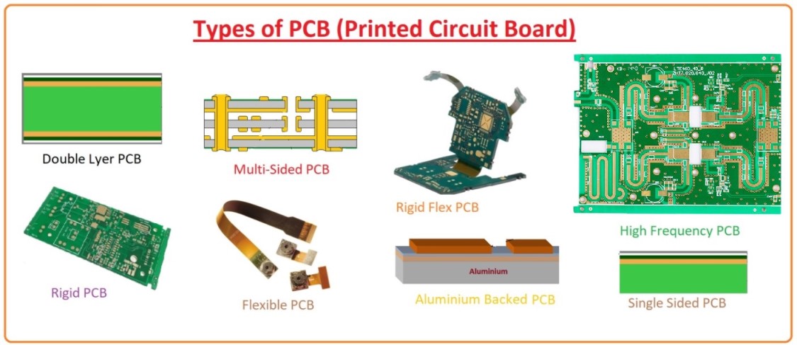
A printed circuit board (PCB) mechanically supports and electrically connects electrical or electronic components using conductive tracks, pads and other features etched from one or more sheet layers of copper laminated onto and/or between sheet layers of a non-conductive substrate. Components are generally soldered onto the PCB to both electrically connect and mechanically fasten them to it.PCBs can be single-sided (one copper layer), double-sided (two copper layers on both sides of one substrate layer), or multi-layer (outer and inner layers of copper, alternating with layers of substrate). Multi-layer PCBs allow for much higher component density, because circuit traces on the inner layers would otherwise take up surface space between components. The rise in popularity of multilayer PCBs with more than two, and especially with more than four, copper planes was concurrent with the adoption of surface mount technology.
YMS Normal PCB manufacturing capabilities:
| YMS Normal PCB manufacturing capabilities overview | ||
| Feature | capabilities | |
| Layer Count | 1-60L | |
| Available Normal PCB Technology | Through hole with Aspect Ratio 16:1 | |
| buried and blind via | ||
| Hybrid | High Frequency Material such as RO4350B and FR4 Mix etc. | |
| High Speed Material such as M7NE and FR4 Mix etc. | ||
| Material | CEM- | CEM-1;CEM-2;CEM-4;CEM-5.etc |
| FR4 | EM827, 370HR, S1000-2, IT180A, IT158, S1000 / S1155, R1566W, EM285, TU862HF,NP170G etc. | |
| High Speed | Megtron6, Megtron4, Megtron7,TU872SLK, FR408HR,N4000-13 Series,MW4000,MW2000,TU933 etc. | |
| High Frequency | Ro3003, Ro3006, Ro4350B, Ro4360G2, Ro4835, CLTE, Genclad, RF35, FastRise27 etc. | |
| Others | Polyimide, Tk, LCP, BT, C-ply, Fradflex, Omega , ZBC2000,PEEK,PTFE,ceramic-based etc. | |
| Thickness | 0.3mm-8mm | |
| Max.copper Thickness | 10OZ | |
| Minimum line Width and Space | 0.05mm/0.05mm(2mil/2mil) | |
| BGA PITCH | 0.35mm | |
| Min mechanical Drilled Size | 0.15mm(6mil) | |
| Aspect Ratio for through hole | 16:1 | |
| Surface Finish | HASL, Lead free HASL,ENIG,Immersion Tin, OSP, Immersion Silver, Gold Finger, Electroplating Hard Gold, Selective OSP,ENEPIG.etc. | |
| Via Fill Option | The via is plated and filled with either conductive or non-conductive epoxy then capped and plated over(VIPPO) | |
| Copper filled, silver filled | ||
| Registration | ±4mil | |
| Solder Mask | Green, Red, Yellow, Blue, White, Black, Purple, Matte Black, Matte green.etc. | |
Product detail pictures:


Related Product Guide:
High Density Interconnect(HDI) PCBs Market Research Methodology Focuses On Exploring Major Factors Influencing the Industry Development 2023 key players IBIDEN Group, Unimicron, AT&S, SEMCO, NCAB Group, Young Poong Group, ZDT, Compeq, Unitech Printed Ci | 1.2m 2layer Led Pcb
HDI PCB Market Expands At A CAGR Of 11.1%, By 2025 Scrutinized In New Research | Copper Base Board
"Based on domestic market and expand abroad business" is our progress strategy for High definition Copper Base Board - PCB bare board 4L Black Soldermask buried Hole PCB| YMS PCB – Yongmingsheng , The product will supply to all over the world, such as: Puerto Rico, Cancun, Cairo, Our company, is always regarding quality as company' s foundation, seeking for development via high degree of credibility , abiding by iso9000 quality management standard strictly , creating top-ranking company by spirit of progress-marking honesty and optimism.
Perfect services, quality products and competitive prices, we have work many times, every time is delighted, wish continue to maintain!


