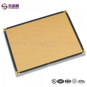
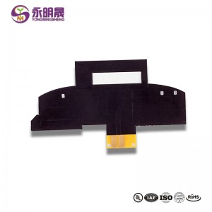
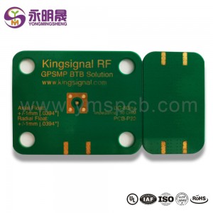
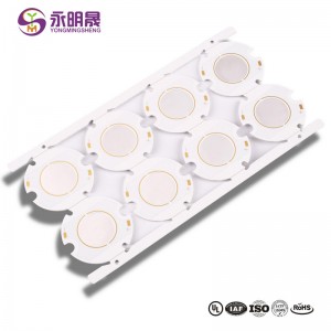
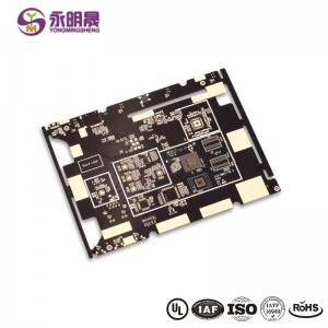
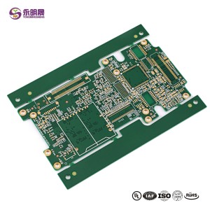
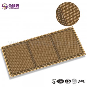
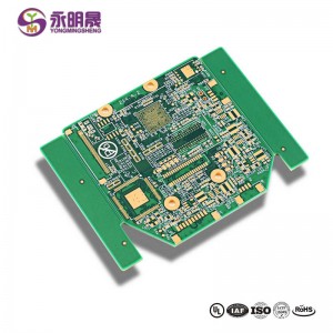
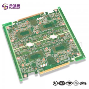
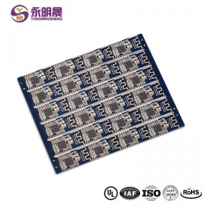
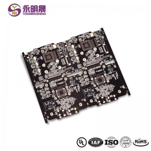
Pākuʻi hōʻike LED pcb HDI laser ma o PAD keleawe pani ʻia | YMSPCB
He aha ka pale LED i i paiia huakai kaapuni a ka papa:
ʻO ka hōʻike LED, ʻike ʻia ʻo ka pale LED, ka pā wikiō LED, ka panela LED a i ʻole nā hōʻailona LED, ua hoʻololi mālie i nā pāleona kuʻuna, nā pahu kukui a pēlā aku me kāna mau pono kū hoʻokahi. Ua lilo ka hoʻolaha hoʻolaha LED i mea ikaika hou i ka ʻoihana media.
Hiki i nā hoʻolaha kuʻuna ke hōʻike wale i nā kiʻi, akā ʻo ka hōʻike LED / hōʻike LED / alakaʻi LED hiki ke lilo i hui piha o nā huaʻōlelo, kiʻi, wikiō a me ke kani, a hiki iā ʻoe ke hoʻololi i ka hōʻike e pono ai.
ʻO ka mea hiki ke hoʻokani maʻalahi ʻia ma o ka hoʻonohonoho ʻana i nā lako polokalamu mea pāʻani, a he kiʻekiʻena kiʻekiʻe, ke aniani kiʻekiʻe a me ke kala piha
Hiki i ka pale hoʻolaha hoʻolaha LED ke ʻumeʻume i ka maka o ka poʻe hele wāwae, a maʻalahi hoʻi e hoʻomanaʻo, hiki ke hana i nā hopena hoʻolaha nui aʻe.
Hoʻohana ākea nā hiʻohiʻona LED i kēia manawa ma ka hoʻolaha pāʻoihana, ka halihali, ka palekana, ka waiwai a me ka hana o ke kahua.
He nani ka hōʻike LED a ʻaʻole maʻalahi maʻalahi, a he lōʻihi kona ola lawelawe, e mālama ai i nā kumukūʻai he nui a me nā lilo.
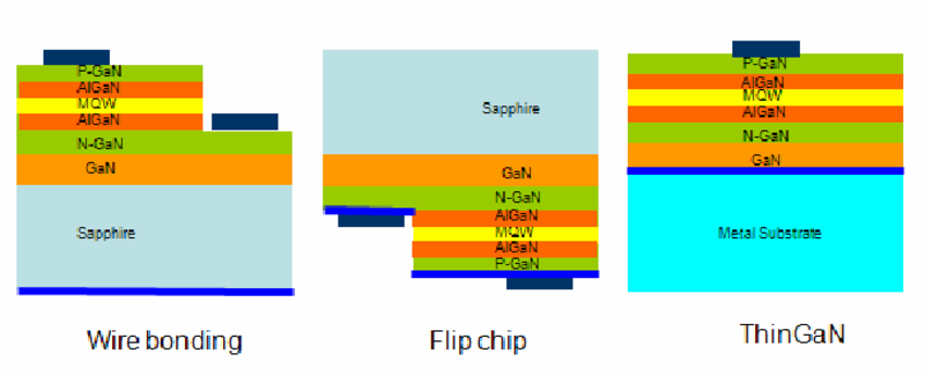
Schematic diagrams of wire bonding flip chip and ThinGaN LEDs
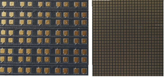
Hōʻike YMS LED i ka pale hana pcb pcb:
| Hōʻike YMS LED hōʻike pcb i ka nānā ʻana i ka hiki ke nānā | |
| Hiʻona | nā hiki |
| Helu Layer | 1-60L |
| Loaʻa LED pale pale pcb ʻenehana | 1 + N + 1 |
| 2 + N + 2 | |
| 3 + N + 3 | |
| 4 + N + 4 | |
| 5 + N + 5 | |
| Kekahi papa | |
| Mānoanoa | 0.3mm-6mm |
| Ka laina liʻiliʻi loa a me ka lewa | 0.05mm / 0.05mm (2mil / 2mil) |
| ʻO Light Emitting Diode PITCH | P0.47mm; P0.58mm; P0.70mm; P0.77mm; P0.925mm; P1.0mm; etc. |
| Min kukuna ʻeli ʻia ka nui | 0.075mm (3nil) |
| Min mīkini ʻeli ka nui | 0.15mm (6mil) |
| Lākiō hiʻohiʻona no ka puka kukuna | 0.9: 1 |
| Lākiō hiʻohiʻona no ma o ka puka | 16: 1 |
| ʻIli Pau | HASL, Alakai manuahi HASL, ENIG, Immersion Tin, OSP, Immersion Silver, Gold Finger, Electroplating Hard Gold, Selective OSP, ENEPIG.etc. |
| Via Hoʻopiha Hoʻopiha | Hoʻopili ʻia ka via a hoʻopiha ʻia me kekahi epoxy conductive a i ʻole non-conductive a laila kāpili ʻia a uhi ʻia i luna |
| Piha keleawe, hoʻopiha kālā | |
| Paʻa ʻia ka laser ma o ke keleawe | |
| Kakau inoa | ± 4milā |
| Makakiʻi paukū | ʻŌmaʻomaʻo, ʻulaʻula, melemele, polū, keʻokeʻo, ʻeleʻele, poni, Matte ʻeleʻele, Matte ʻōmaʻomaʻo. |
- It is beneficial to use LED PCB as it helps electronics get thinner and smaller. Its numerous applications include but not limited to:
-
1. Telecom LED PCB
Telecommunication devices use LED displays and indicators. The LEDs offer decreased weight, improved durability, and enhanced heat transfer. So, they are much useful in the telecom sector applications such as high-frequency amplifiers and filtering appliances.
-
2. Automotive LED PCB
They can be found in car indicators, brake lights, headlights, and other devices. Longevity, durability, and low prices are the reason that LED PCBs aluminum PCB are common in the automotive industry.
-
3. Computer LED PCB
They are also becoming common in computer equipment as indicators and displays. The LED PCB board is an ideal solution for the heat-sensitive computer machinery.
-
4. Medical LED PCB
In medical examinations and surgeries, high-powered LED lighting tools are used. They ensure the proper function of the medical equipment regardless of the number of patients in the medical office.
-
5. Other LED PCB
Other application fields of LED PCB board are airport runway lights, street lighting, photovoltaic (solar) lightening, lanterns and flashlights, highway tunnel lightening, highway growth plant, signal, and traffic lighting.
LED PCBs are best for consumer devices, some marine and aviation applications, flashlight and other camping accessories in lower-light environments, elevator lighting, power converters, decorative and concealed lights, and many more
E aʻo hou aʻe e pili ana i nā huahana YMS


