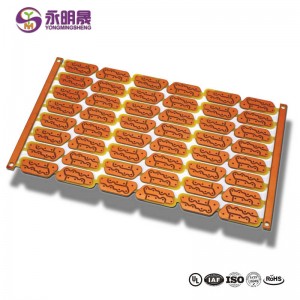
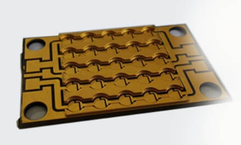
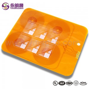
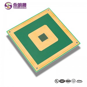
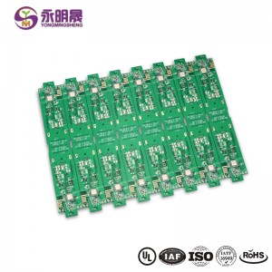
Extreme Copper PCB 2 Layer 10 0z Heavy Copper Board| YMS PCB
The construction of a heavy copper circuit endows a board with benefits such as:
- Increased endurance to thermal strains.
- Increased current carrying capacity.
- Increased mechanical strength at connector sites and in PTH holes.
- Use of exotic materials to their full potential without circuit failure.
- Reduced product size by incorporating multiple copper weights on the same layer of circuitry .
- Heavy copper plated vias carry higher current through the board and help to transfer heat to an external heatsink.
ʻO YMS Heavy copper PCB nā mana hana:
| ʻO YMS Heavy copper PCB manufacturing hiki ke nānā aku | ||
| Hiʻona | nā hiki | |
| Helu Layer | 1-30L | |
| Nā Pono Hana | FR-4 Tg maʻamau, FR4-waena Tg,FR4-Tg kiʻekiʻe | |
| Mānoanoa | 0.6 mm - 8.0mm | |
| Kaumaha Copper Layer Mawaho (Hoʻopau) | 15OZ | |
| ʻO ke kaumaha keleawe o loko (Hoʻopau) | 30OZ | |
| Ka laina liʻiliʻi loa a me ka lewa | 4oz Cu 8mil/8mil; 5oz Cu 10mil/10mil; 6oz Cu 12mil/12mil; 12oz Cu 18mil/28mil; 15oz Cu 30mil/38mil .etc. | |
| BGA PITCH | 0.8mm (32mil) | |
| Min mīkini ʻeli ka nui | 0.25mm (10mil) | |
| Lākiō hiʻohiʻona no ma o ka puka | 16 : 1 | |
| ʻIli Pau | HASL, Alakai manuahi HASL, ENIG, Immersion Tin, OSP, Immersion Silver, Gold Finger, Electroplating Hard Gold, Selective OSP, ENEPIG.etc. | |
| Via Hoʻopiha Hoʻopiha | Hoʻopili ʻia ka via a hoʻopihapiha ʻia me kekahi epoxy conductive a i ʻole non-conductive a laila kāpili ʻia a plated ma luna (VIPPO) | |
| Piha keleawe, hoʻopiha kālā | ||
| Kakau inoa | ± 4milā | |
| Makakiʻi paukū | ʻŌmaʻomaʻo, ʻulaʻula, melemele, polū, keʻokeʻo, ʻeleʻele, poni, Matte ʻeleʻele, Matte ʻōmaʻomaʻo. | |
Makemake ʻoe:
1、What are the precautions for heavy copper PCB wiring
2、What are the specifications of heavy copper PCB
3、What are the heavy copper PCB materials
E aʻo hou aʻe e pili ana i nā huahana YMS


E kākau i kou manaʻo ma 'aneʻi, a hoouna aku ia ia mai

