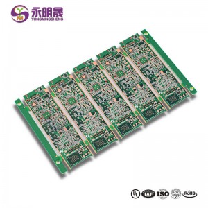
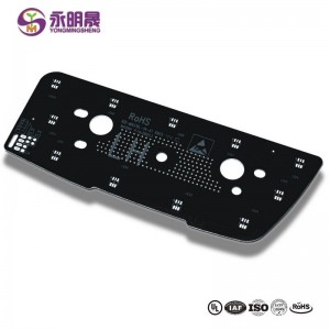
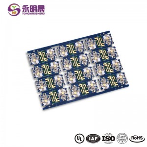
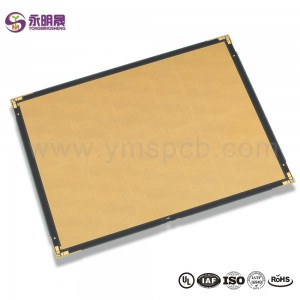
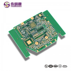
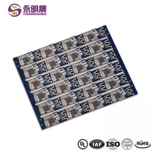
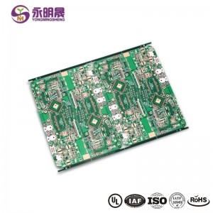
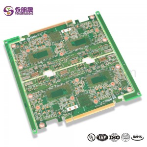
HDI PCB 12 Layer 2 Step HDI Board | YMS PCB
kiko'î
Papa: 12
Base Material:FR4 High Tg EM827
Mānoanoa: 1.2 ± 0.1mm
Min.Hole Size:0.15mm
Minimum Line Width/Space:0.075mm/0.075mm
Ka ʻoluʻolu liʻiliʻi ma waena o ka papa o ka hohonu PTH a me ka laina: 0.2mm
Size:101mm×55mm
Lākiō hiʻohiʻona: 8: 1
ʻIlikai lapaʻau: ENIG
Speciality: Laser via copper plated shut,VIPPO Technology,Blind Via and Buried Hole
Noi: kelekaʻaʻike
What is HDI PCBs?
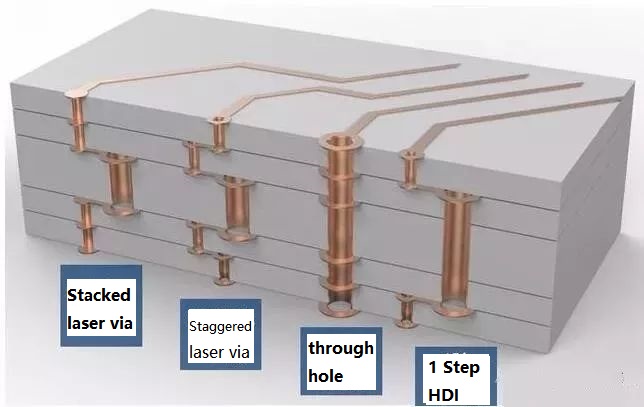
High density interconnect (HDI) PCBs represent one of the fastest-growing segments of the printed circuit board market. Because of its higher circuitry density, the ʻO HDI PCB ka PCB design can incorporate finer lines and spaces, smaller vias and capture pads, and higher connection pad densities. A high-density PCB features blind and buried vias and often contains microvias that are .006 in diameter or even less.
1.Multi-ʻanuʻu HDI mau hiʻohiʻona nō i ka pilina ma waena o kekahi papa;
2.Cross-, ahu iho kukuna aaioee hiki ka hōʻoi 'i ka pono nui o ka nunui-ʻanuʻu HDI;
3.The me ka hui pu ana o HDI a me kiʻekiʻe-alapine (frequency) kumuhana, metala-ma muli laminates, FPC a me nā kūikawā laminates a me keʻano o ka hanaʻana hiki ai i na mea e pono ai o kiʻekiʻe nuʻa a me kiʻekiʻe alapine (frequency), kiʻekiʻe ka wela 'ana i lawelawe, a me 3Dʻaha kanaka.
Hana ʻo YMS HDI PCB hana capa :
| ʻO YMS HDI PCB hana hana nānā ākea | |
| Hiʻona | nā hiki |
| Helu Layer | 4-60L |
| Loaʻa HDI ʻenehana HDB | 1 + N + 1 |
| 2 + N + 2 | |
| 3 + N + 3 | |
| 4 + N + 4 | |
| 5 + N + 5 | |
| Kekahi papa | |
| Mānoanoa | 0.3mm-6mm |
| Ka laina liʻiliʻi loa a me ka lewa | 0.05mm / 0.05mm (2mil / 2mil) |
| BGA PITCH | 0.35mm |
| Min kukuna ʻeli ʻia ka nui | 0.075mm (3nil) |
| Min mīkini ʻeli ka nui | 0.15mm (6mil) |
| Lākiō hiʻohiʻona no ka puka kukuna | 0.9: 1 |
| Lākiō hiʻohiʻona no ma o ka puka | 16: 1 |
| ʻIli Pau | HASL, Alakai manuahi HASL, ENIG, Immersion Tin, OSP, Immersion Silver, Gold Finger, Electroplating Hard Gold, Selective OSP, ENEPIG.etc. |
| Via Hoʻopiha Hoʻopiha | Hoʻopili ʻia ka via a hoʻopiha ʻia me kekahi epoxy conductive a i ʻole non-conductive a laila kāpili ʻia a uhi ʻia i luna |
| Piha keleawe, hoʻopiha kālā | |
| Paʻa ʻia ka laser ma o ke keleawe | |
| Kakau inoa | ± 4milā |
| Makakiʻi paukū | ʻŌmaʻomaʻo, ʻulaʻula, melemele, polū, keʻokeʻo, ʻeleʻele, poni, Matte ʻeleʻele, Matte ʻōmaʻomaʻo. |
Makemake ʻoe:
1, The application range and circuit advantage of HDI board are introduced
2、PCB production skills: HDI board CAM production method
3、PCB design of 1 step, 2 step and 3step HDI
5、Ma hea kahi i hoʻohana ʻia ai nā PCB HDI
E aʻo hou aʻe e pili ana i nā huahana YMS


What is HDI in PCB?
HDI Boards – High Density Interconnect
What are the layers of a PCB?
Substrate Layer.
Copper Layer.
Soldermask layer.
Silkscreen layer.
What is HDI stackup?
HDI is short for high density interconnect, and refers to the use of buried, blind and micro vias as well as any layer HDIs to create compact boards.

