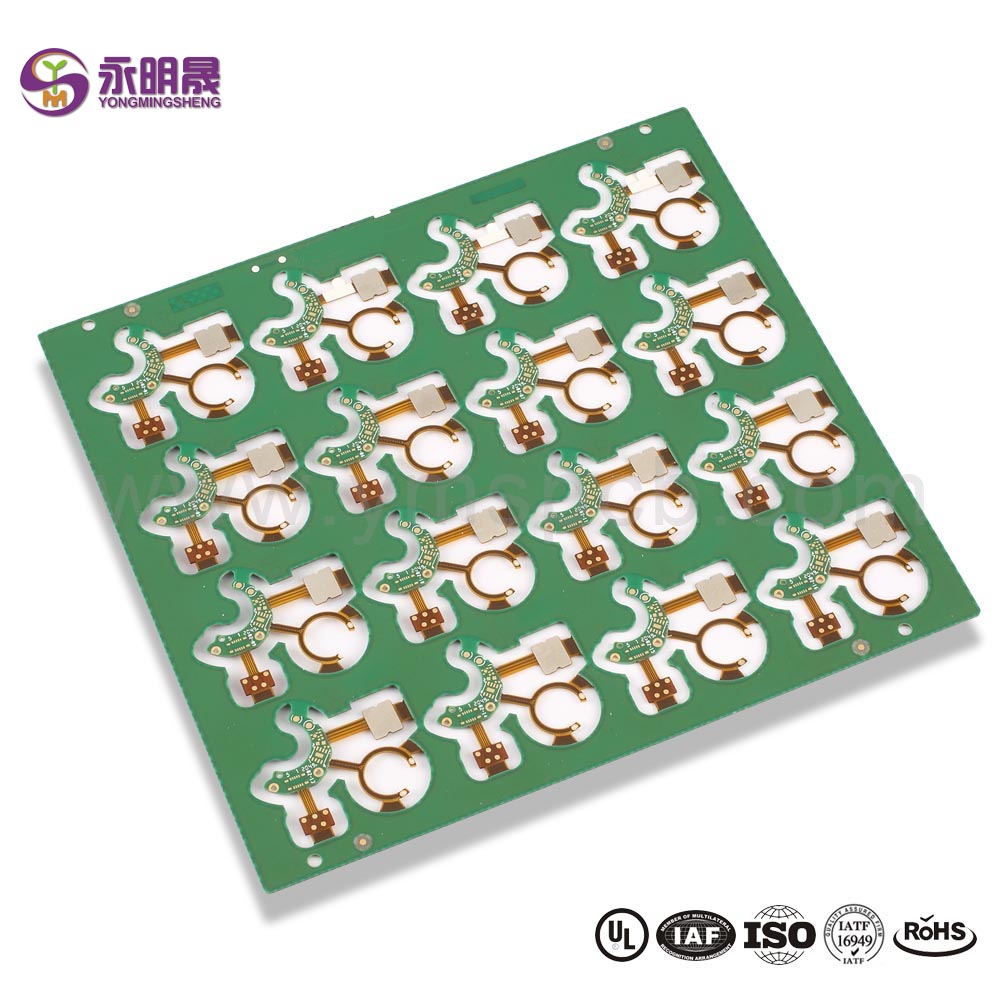
Double sided pcb Normal pcb Lead free HASL Counterbore Manufacturer | YMS PCB
HAL(Lead Free), the full name is Hot Air leveling with Lead Free. Compared with HASL, the main difference for HAL(Lead Free) is the element of material which do not contain Lead(Pb), so it’s RoHS Compliant and it’s much more popular and widely used in PCB na .
HAL(Lead Free) requires higher run temperatures for lead free solder and longer contact time, the production cost for HAL(Lead Free) is slightly higher than HASL(Tin/Lead).
The manufacturing process of HAL(Lead Free) is similar to HASL(Tin/Lead), the circuit boards will be submersed in molten solder(Lead Free). This solder will cover all the exposed copper surfaces. Upon retraction from the solder, high pressure hot air is blown over the surface through air knives, this levels the solder deposit and removes the excess solder from the surface of printed circuit boards.
Gabatarwar Da'irar Hukumar Gabatarwa
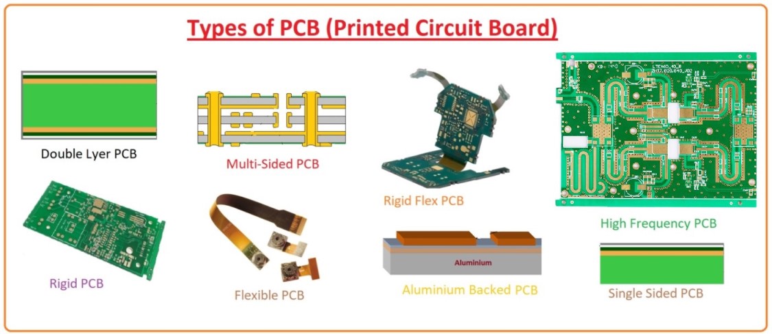
Hukumar da'ira Buga ta al'ada: Most PCBs for simple electronics are simple and composed of only a single layer. More sophisticated hardware such as computer graphics cards or motherboards can have 2 or multiple layers, sometimes up to twelve.
A printed circuit board (PCB) mechanically supports and electrically connects electrical or electronic components using conductive tracks, pads and other features etched from one or more sheet layers of copper laminated onto and/or between sheet layers of a non-conductive substrate. Components are generally soldered onto the PCB to both electrically connect and mechanically fasten them to it.PCBs can be single-sided (one copper layer), double-sided (two copper layers on both sides of one substrate layer), or multi-layer (outer and inner layers of copper, alternating with layers of substrate). Multi-layer PCBs allow for much higher component density, because circuit traces on the inner layers would otherwise take up surface space between components. The rise in popularity of multilayer PCBs with more than two, and especially with more than four, copper planes was concurrent with the adoption of surface mount technology.
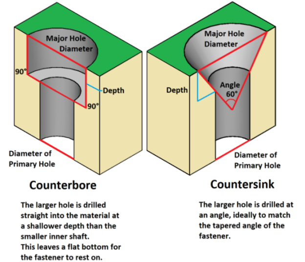
What is the difference between a Countersink and a Counterbore?
YMS Al'ada PCB masana'antu damar:
| YMS Al'ada PCB masana'antu damar overview | ||
| Fasali | damar | |
| Countididdigar Layer | 1-60L | |
| Akwai Fasaha na PCB na al'ada | Ta hanyar rami tare da Tsarin 16: 1 | |
| binne shi da makafi via | ||
| Matattara | Babban Yanayin Yanayi kamar RO4350B da FR4 Mix da dai sauransu. | |
| Babban abu mai sauri kamar M7NE da FR4 Mix da dai sauransu. | ||
| Kayan aiki | CEM- | CEM-1; CEM-2 ; CEM-4 ; CEM-5.da sauransu |
| FR4 | EM827, 370HR, S1000-2, IT180A, IT158, S1000 / S1155, R1566W, EM285, TU862HF, NP170G da dai sauransu | |
| high Speed | Megtron6, Megtron4, Megtron7, TU872SLK, FR408HR, N4000-13 Series, MW4000, MW2000, TU933 da dai sauransu | |
| high Frequency | Ro3003, Ro3006, Ro4350B, Ro4360G2, Ro4835, CLTE, Genclad, RF35, FastRise27 da dai sauransu. | |
| Sauran | Polyimide, Tk, LCP, BT, C-ply, Fradflex, Omega, ZBC2000, PEEK, PTFE, yumbu da sauransu. | |
| Kauri | 0.3mm-8mm | |
| Max.copper Kauri | 10 OZ | |
| Ananan Layin Faɗi da Sarari | 0.05mm / 0.05mm (2mil / 2mil) | |
| FITAR BGA | 0.35mm | |
| Min Girman Hannun injina | 0.15mm (6mil) | |
| Ra'ayin ƙasa don rami | 16 : 1 | |
| Gama Gama | HASL, Jagora kyauta HASL, ENIG, Nitsar da Tin, OSP, Azurfar Nutsewa, Yatsan Zinare, Gyara Zinariya Mai Wuya, Mai Zaba OSP , ENEPIG.etc. | |
| Ta Hanyar Cika zaɓi | An saka abin da ke ciki kuma an cika shi da mai sarrafawa ko wanda ba shi da wata ma'amala sannan a rufe shi kuma ya rufe (VIPPO) | |
| An cika tagulla, an cika azurfa | ||
| Rijista | ± 4mil | |
| Masassarar Solder | Kore, Ja, Rawaya, Shuɗi, Fari, Baƙi, Mai Tsara, Matta Baki, Matte kore. Da dai sauransu. | |
Kuna Iya So:
1. Summary of matters needing attention in circuit board welding
3. What is PCB
Ƙara koyo game da samfuran YMS


