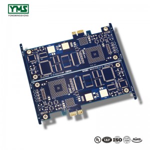
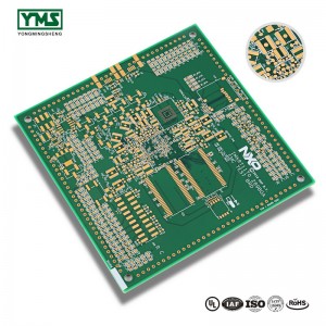
YMS offers Rapid PCB Prototyping for Your Research Work
YMS offers Rapid PCB Prototyping for Your Research Work
PCB prototyping used to the nightmares of many electronics professionals. YMS now terminates the nightmares! We can get your first-try boards right in 48 hours!
Prototyping stage is the most critical period of time for engineers, students and hobbyists. YMS not only makes your boards quick, but also makes your job right as well as cost-effective. This greatly reduces your cost and shorten the time for developing your electronic products.
The portfolio of PCBs we produce contains a broad variety of products; from 2L PCBs to highly advanced HDI and flex boards. Even though the PCBs we produce differ a lot regarding functionality and areas of use, they all have one thing in common. The common denominator for all PCBs is that our experts oversee that the production – from prototyping up to volume – is working according to our processes and product specification.
Having been in the PCB industry for 11 years, YMS prides itself as one of leading suppliers of PCB prototyping and low-volume production in the world. Our turn time can be as short as 24 hours after your Gerber files being reviewed and approved by our engineers, greatly saving you time in your work.
You may choose other time schedules to fit your budget, if your work timeframe is not that tight. We offer 48-hours and 72-hours shipping too.
Being quick in delivery never compromises on the quality. With our stringent test procedures, you can be assured that you will be satisfied with our PCB for your high-tech work. Apart from the quality, we can almost beat every other fabricators on prices, which is critical for your work as you may need tens of hundreds of PCBs to finalize your research and design.
We shorten the delivery time while guarantee quality,produced by chemical processes for pads and vias metallization,Refuse conductive adhesive technology to save costs ,each order must go through 70 minutes copper plating,AOI and probe test,and we take advantage of internationally known base materials.
In addition to the reduction in lead time, YMS not only reduced the price of small batch PCB,but also the freight cost for DHL parcels below 1 KG.
YMS Normal PCB manufacturing capabilities:
| YMS Normal PCB manufacturing capabilities overview | ||
| Feature | capabilities | |
| Layer Count | 1-60L | |
| Available Normal PCB Technology | Through hole with Aspect Ratio 16:1 | |
| buried and blind via | ||
| Hybrid | High Frequency Material such as RO4350B and FR4 Mix etc. | |
| High Speed Material such as M7NE and FR4 Mix etc. | ||
| Material | CEM- | CEM-1;CEM-2;CEM-4;CEM-5.etc |
| FR4 | EM827, 370HR, S1000-2, IT180A, IT158, S1000 / S1155, R1566W, EM285, TU862HF,NP170G etc. | |
| High Speed | Megtron6, Megtron4, Megtron7,TU872SLK, FR408HR,N4000-13 Series,MW4000,MW2000,TU933 etc. | |
| High Frequency | Ro3003, Ro3006, Ro4350B, Ro4360G2, Ro4835, CLTE, Genclad, RF35, FastRise27 etc. | |
| Others | Polyimide, Tk, LCP, BT, C-ply, Fradflex, Omega , ZBC2000,PEEK,PTFE,ceramic-based etc. | |
| Thickness | 0.3mm-8mm | |
| Max.copper Thickness | 10OZ | |
| Minimum line Width and Space | 0.05mm/0.05mm(2mil/2mil) | |
| BGA PITCH | 0.35mm | |
| Min mechanical Drilled Size | 0.15mm(6mil) | |
| Aspect Ratio for through hole | 16:1 | |
| Surface Finish | HASL, Lead free HASL,ENIG,Immersion Tin, OSP, Immersion Silver, Gold Finger, Electroplating Hard Gold, Selective OSP,ENEPIG.etc. | |
| Via Fill Option | The via is plated and filled with either conductive or non-conductive epoxy then capped and plated over(VIPPO) | |
| Copper filled, silver filled | ||
| Registration | ±4mil | |
| Solder Mask | Green, Red, Yellow, Blue, White, Black, Purple, Matte Black, Matte green.etc. | |


