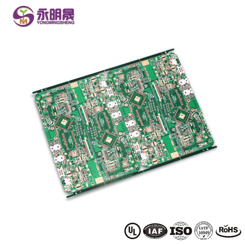
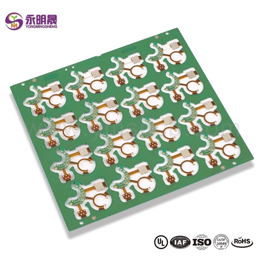
Double sided pcb Normal pcb Lead free HASL Counterbore Manufacturer | YMS PCB
HAL(Lead Free), the full name is Hot Air leveling with Lead Free. Compared with HASL, the main difference for HAL(Lead Free) is the element of material which do not contain Lead(Pb), so it’s RoHS Compliant and it’s much more popular and widely used in e .
HAL(Lead Free) requires higher run temperatures for lead free solder and longer contact time, the production cost for HAL(Lead Free) is slightly higher than HASL(Tin/Lead).
The manufacturing process of HAL(Lead Free) is similar to HASL(Tin/Lead), the circuit boards will be submersed in molten solder(Lead Free). This solder will cover all the exposed copper surfaces. Upon retraction from the solder, high pressure hot air is blown over the surface through air knives, this levels the solder deposit and removes the excess solder from the surface of printed circuit boards.
Introduzione à u Circuitu Stampatu
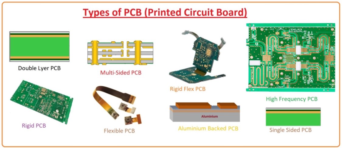
Circuitu stampatu normale: Most PCBs for simple electronics are simple and composed of only a single layer. More sophisticated hardware such as computer graphics cards or motherboards can have 2 or multiple layers, sometimes up to twelve.
A printed circuit board (PCB) mechanically supports and electrically connects electrical or electronic components using conductive tracks, pads and other features etched from one or more sheet layers of copper laminated onto and/or between sheet layers of a non-conductive substrate. Components are generally soldered onto the PCB to both electrically connect and mechanically fasten them to it.PCBs can be single-sided (one copper layer), double-sided (two copper layers on both sides of one substrate layer), or multi-layer (outer and inner layers of copper, alternating with layers of substrate). Multi-layer PCBs allow for much higher component density, because circuit traces on the inner layers would otherwise take up surface space between components. The rise in popularity of multilayer PCBs with more than two, and especially with more than four, copper planes was concurrent with the adoption of surface mount technology.
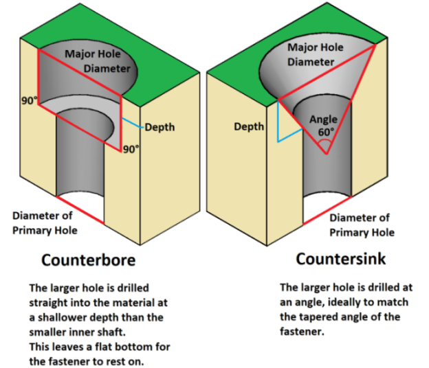
What is the difference between a Countersink and a Counterbore?
Capacità di fabricazione normale di YMS PCB:
| Panoramica di capacità di fabbricazione PCB YMS Normale | ||
| Feature | capacità | |
| Conti di Livelli | 1-60 l | |
| Disponibile Tecnulugia PCB Normale | Foru attraversu cù Proporzione 16: 1 | |
| sipoltu è cecu via | ||
| Ibridu | Materiale Alta Frequenza cume RO4350B è FR4 Mix ecc. | |
| Materiale à Alta Velocità cum'è M7NE è FR4 Mix ecc. | ||
| Materiale | CEM- | CEM-1; CEM-2 ; CEM-4 ; CEM-5.etc |
| FR4 | EM827, 370HR, S1000-2, IT180A, IT158, S1000 / S1155, R1566W, EM285, TU862HF, NP170G etc. | |
| Alta Velocità | Megtron6, Megtron4, Megtron7, TU872SLK, FR408HR, N4000-13 Series, MW4000, MW2000, TU933 etc. | |
| Alta Frequenza | Ro3003, Ro3006, Ro4350B, Ro4360G2, Ro4835, CLTE, Genclad, RF35, FastRise27 etc. | |
| Altri | Polyimide, Tk, LCP, BT, C-ply, Fradflex, Omega, ZBC2000, PEEK, PTFE, basatu in ceramica etc. | |
| Spessore | 0,3 mm-8 mm | |
| Spessore Rame Max | 10 OZ | |
| Larghezza minima di linea è Spaziu | 0.05mm / 0.05mm (2mil / 2mil) | |
| BGA PITCH | 0,35 mm | |
| Dimensione minima forata meccanica | 0.15mm (6mil) | |
| Ratio d'aspettu per u foru passante | 16 : 1 | |
| Finitura superficiale | HASL, HASL senza piombu, ENIG, Stagnu à immersione, OSP, Argentu à immersione, Dita d'oru, Galvanoplastia Duro Duro, OSP selettivu E ENEPIG.etc. | |
| Via Opzione Fill | A via hè placcata è piena di epossidia cunduttiva o non conduttiva poi tappata è placcata (VIPPO) | |
| Rame pienu, argentu pienu | ||
| Scrizzione | ± 4mil | |
| Maschera di Saldatura | Verde, Rossu, Giallu, Turchinu, Biancu, Neru, Viulettu, Neru Matteu, verde Matteu ecc. | |
Puderete Piace:
1 、Summary of matters needing attention in circuit board welding
3 、What is PCB
4、Cosa hè a prova à bordu nudu?
5. Chì ghjè u disignu di PCB d'alta frequenza
Amparate più nantu à i prudutti YMS


